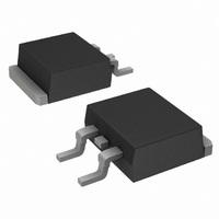
NTB30N20T4G ON Semiconductor, NTB30N20T4G Datasheet - Page 5

NTB30N20T4G
Manufacturer Part Number
NTB30N20T4G
Description
MOSFET N-CH 200V 30A D2PAK
Manufacturer
ON Semiconductor
Datasheet
1.NTB30N20T4G.pdf
(8 pages)
Specifications of NTB30N20T4G
Fet Type
MOSFET N-Channel, Metal Oxide
Fet Feature
Standard
Rds On (max) @ Id, Vgs
81 mOhm @ 15A, 10V
Drain To Source Voltage (vdss)
200V
Current - Continuous Drain (id) @ 25° C
30A
Vgs(th) (max) @ Id
4V @ 250µA
Gate Charge (qg) @ Vgs
100nC @ 10V
Input Capacitance (ciss) @ Vds
2335pF @ 25V
Power - Max
2W
Mounting Type
Surface Mount
Package / Case
D²Pak, TO-263 (2 leads + tab)
Configuration
Single
Transistor Polarity
N-Channel
Resistance Drain-source Rds (on)
0.081 Ohm @ 10 V
Forward Transconductance Gfs (max / Min)
20 S
Drain-source Breakdown Voltage
200 V
Gate-source Breakdown Voltage
+/- 30 V
Continuous Drain Current
30 A
Power Dissipation
214000 mW
Maximum Operating Temperature
+ 175 C
Mounting Style
SMD/SMT
Minimum Operating Temperature
- 55 C
Lead Free Status / RoHS Status
Lead free / RoHS Compliant
Other names
NTB30N20T4GOS
NTB30N20T4GOS
NTB30N20T4GOSTR
NTB30N20T4GOS
NTB30N20T4GOSTR
Available stocks
Company
Part Number
Manufacturer
Quantity
Price
Company:
Part Number:
NTB30N20T4G
Manufacturer:
ON
Quantity:
1 600
Company:
Part Number:
NTB30N20T4G
Manufacturer:
ON
Quantity:
12 500
the maximum simultaneous drain−to−source voltage and
drain current that a transistor can handle safely when it is
forward biased. Curves are based upon maximum peak
junction temperature and a case temperature (T
Peak repetitive pulsed power limits are determined by using
the thermal response data in conjunction with the procedures
discussed
Resistance−General Data and Its Use.”
traverse any load line provided neither rated peak current
(I
transition time (t
power averaged over a complete switching cycle must not
exceed (T
in switching circuits with unclamped inductive loads. For
DM
10
The Forward Biased Safe Operating Area curves define
Switching between the off−state and the on−state may
A Power MOSFET designated E−FET can be safely used
12
8
6
4
2
0
0
Figure 8. Gate−To−Source and Drain−To−Source
) nor rated voltage (V
V
DS
J(MAX)
Q
10
1
in
Voltage versus Total Charge
Q
r
,t
G
− T
f
) do not exceed 10 ms. In addition the total
20
, TOTAL GATE CHARGE (nC)
C
AN569,
)/(R
30
qJC
Q
).
Q
DSS
T
2
40
DRAIN−TO−SOURCE DIODE CHARACTERISTICS
) is exceeded and the
30
25
20
15
10
“Transient
5
0
0.5
Figure 10. Diode Forward Voltage versus Current
V
T
50
GS
J
V
= 25°C
SD
= 0 V
, SOURCE−TO−DRAIN VOLTAGE (VOLTS)
I
T
D
0.6
J
SAFE OPERATING AREA
C
= 30 A
= 25°C
60
) of 25°C.
V
Thermal
GS
http://onsemi.com
NTB30N20
70
0.7
180
150
120
90
60
30
0
5
reliable operation, the stored energy from circuit inductance
dissipated in the transistor while in avalanche must be less
than the rated limit and adjusted for operating conditions
differing from those specified. Although industry practice is
to rate in terms of energy, avalanche energy capability is not
a constant. The energy rating decreases non−linearly with an
increase of peak current in avalanche and peak junction
temperature.
drain−to−source avalanche at currents up to rated pulsed
current (I
continuous current (I
The energy rating must be derated for temperature as shown
in the accompanying graph (Figure 12). Maximum energy at
currents below rated continuous I
equal the values indicated.
1000
100
0.8
Although many E−FETs can withstand the stress of
10
1
1
V
I
V
D
DM
DD
GS
= 30 A
t
Figure 9. Resistive Switching Time
d(off)
0.9
Variation versus Gate Resistance
t
), the energy rating is specified at rated
= 160 V
= 10 V
d(on)
t
r
R
G
D
, GATE RESISTANCE (W)
), in accordance with industry custom.
t
f
1
10
D
can safely be assumed to
100


