IRF610STRR Vishay, IRF610STRR Datasheet - Page 5
IRF610STRR
Manufacturer Part Number
IRF610STRR
Description
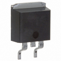
MOSFET N-CH 200V 3.3A D2PAK
Manufacturer
Vishay
Datasheet
1.IRF610S.pdf
(8 pages)
Specifications of IRF610STRR
Fet Type
MOSFET N-Channel, Metal Oxide
Fet Feature
Standard
Rds On (max) @ Id, Vgs
1.5 Ohm @ 2A, 10V
Drain To Source Voltage (vdss)
200V
Current - Continuous Drain (id) @ 25° C
3.3A
Vgs(th) (max) @ Id
4V @ 250µA
Gate Charge (qg) @ Vgs
8.2nC @ 10V
Input Capacitance (ciss) @ Vds
140pF @ 25V
Power - Max
3W
Mounting Type
Surface Mount
Package / Case
D²Pak, TO-263 (2 leads + tab)
Lead Free Status / RoHS Status
Contains lead / RoHS non-compliant


Document Number: 91024
S09-0071-Rev. A, 02-Feb-09
Vary t
required I
91024_09
Fig. 9 - Maximum Drain Current vs. Case Temperature
p
Fig. 12a - Unclamped Inductive Test Circuit
to obtain
4.0
3.0
2.0
1.0
0.0
91024_11
AS
25
R
10 V
G
10
0.1
10
-2
1
V
10
DS
50
0.05
0.02
0.01
-5
T
0 − 0.5
0.2
0.1
C
t
, Case Temperature (°C)
p
Fig. 11 - Maximum Effective Transient Thermal Impedance, Junction-to-Case
75
I
AS
D.U.T
0.01 Ω
10
L
100
-4
Single Pulse
(Thermal Response)
125
10
+
-
t
150
-3
V
1
, Rectangular Pulse Duration (s)
DD
10
-2
Fig. 12b - Unclamped Inductive Waveforms
V
I
90 %
10 %
AS
Fig. 10a - Switching Time Test Circuit
Fig. 10b - Switching Time Waveforms
DS
V
V
DS
0.1
GS
R
Pulse width ≤ 1 µs
Duty factor ≤ 0.1 %
G
10 V
V
GS
t
d(on)
V
Notes:
1. Duty Factor, D = t
2. Peak T
IRF610S, SiHF610S
DS
t
r
t
p
1
j
= P
P
D.U.T.
DM
DM
Vishay Siliconix
R
x Z
D
t
d(off)
t
V
1
1
thJC
/t
DS
2
t
+ T
2
t
f
V
C
+
-
10
www.vishay.com
DD
V
DD
5
Related parts for IRF610STRR
Image
Part Number
Description
Manufacturer
Datasheet
Request
R

Part Number:
Description:
MOSFET N-CH 200V 3.3A D2PAK
Manufacturer:
Vishay
Datasheet:

Part Number:
Description:
MOSFET N-CH 200V 3.3A TO-220AB
Manufacturer:
Vishay
Datasheet:

Part Number:
Description:
357-036-542-201 CARDEDGE 36POS DL .156 BLK LOPRO
Manufacturer:
Vishay
Datasheet:
Part Number:
Description:
357-036-542-201 CARDEDGE 36POS DL .156 BLK LOPRO
Manufacturer:
Vishay
Datasheet:
Part Number:
Description:
357-036-542-201 CARDEDGE 36POS DL .156 BLK LOPRO
Manufacturer:
Vishay
Datasheet:
Part Number:
Description:
357-036-542-201 CARDEDGE 36POS DL .156 BLK LOPRO
Manufacturer:
Vishay
Datasheet:
Part Number:
Description:
357-036-542-201 CARDEDGE 36POS DL .156 BLK LOPRO
Manufacturer:
Vishay
Datasheet:
Part Number:
Description:
357-036-542-201 CARDEDGE 36POS DL .156 BLK LOPRO
Manufacturer:
Vishay
Datasheet:
Part Number:
Description:
357-036-542-201 CARDEDGE 36POS DL .156 BLK LOPRO
Manufacturer:
Vishay
Datasheet:
Part Number:
Description:
357-036-542-201 CARDEDGE 36POS DL .156 BLK LOPRO
Manufacturer:
Vishay
Datasheet:
Part Number:
Description:
357-036-542-201 CARDEDGE 36POS DL .156 BLK LOPRO
Manufacturer:
Vishay
Datasheet:
Part Number:
Description:
357-036-542-201 CARDEDGE 36POS DL .156 BLK LOPRO
Manufacturer:
Vishay
Datasheet:
Part Number:
Description:
357-036-542-201 CARDEDGE 36POS DL .156 BLK LOPRO
Manufacturer:
Vishay
Datasheet:
Part Number:
Description:
357-036-542-201 CARDEDGE 36POS DL .156 BLK LOPRO
Manufacturer:
Vishay
Datasheet:
Part Number:
Description:
357-036-542-201 CARDEDGE 36POS DL .156 BLK LOPRO
Manufacturer:
Vishay
Datasheet: