IRFR9N20DTR International Rectifier, IRFR9N20DTR Datasheet
IRFR9N20DTR
Specifications of IRFR9N20DTR
Available stocks


Related parts for IRFR9N20DTR


IRFR9N20DTR Summary of contents
Page 1
Applications High frequency DC-DC converters Benefits Low Gate-to-Drain Charge to Reduce Switching Losses Fully Characterized Capacitance Including Effective C to Simplify Design, (See OSS App. Note AN1001) Fully Characterized Avalanche Voltage and Current Absolute Maximum Ratings Parameter ...
Page 2
IRFR9N20D/IRFU9N20D Static @ T = 25°C (unless otherwise specified) J Parameter V Drain-to-Source Breakdown Voltage (BR)DSS Breakdown Voltage Temp. Coefficient (BR)DSS J R Static Drain-to-Source On-Resistance DS(on) V Gate Threshold Voltage GS(th) I Drain-to-Source Leakage Current DSS ...
Page 3
VGS TOP 15V 12V 10V 8.0V 7.0V 6.5V 6.0V BOTTOM 5. 20µs PULSE WIDTH 0.1 0 Drain-to-Source Voltage (V) DS Fig 1. Typical Output Characteristics 100 10 ° ...
Page 4
IRFR9N20D/IRFU9N20D 10000 0V, C iss = rss = oss = 1000 Ciss 100 Coss Crss ...
Page 5
T , Case Temperature ( C) C Fig 9. Maximum Drain Current Vs. Case Temperature 0.50 0.20 0.10 0.05 0.1 0.02 SINGLE PULSE 0.01 (THERMAL ...
Page 6
IRFR9N20D/IRFU9N20D Fig 12a. Unclamped Inductive Test Circuit Fig 12b. Unclamped ...
Page 7
D.U Driver Gate Drive P.W. D.U.T. I Waveform SD Reverse Recovery Current D.U.T. V Waveform DS Re-Applied Voltage Inductor Curent * for Logic Level Devices GS Fig 14. For N-Channel HEXFET www.irf.com IRFR9N20D/IRFU9N20D ...
Page 8
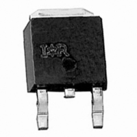
IRFR9N20D/IRFU9N20D D-Pak (TO-252AA) Package Outline Dimensions are shown in millimeters (inches (. (. (. (.2 0 ...
Page 9
I-Pak (TO-251AA) Package Outline Dimensions are shown in millimeters (inches (. (. (. (. ...
Page 10
IRFR9N20D/IRFU9N20D D-Pak (TO-252AA) Tape & Reel Information Dimensions are shown in millimeters (inches 12 11 LLIN G ...
Page 11
Note: For the most current drawings please refer to the IR website at: http://www.irf.com/package/ ...