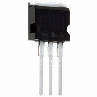
STB16NK65Z-S STMicroelectronics, STB16NK65Z-S Datasheet

STB16NK65Z-S
Specifications of STB16NK65Z-S
Available stocks
Related parts for STB16NK65Z-S
STB16NK65Z-S Summary of contents
Page 1
... IDEAL FOR OFF-LINE POWER SUPPLIES Table 2: Order Codes SALES TYPE STP16NK65Z STB16NK65Z-S September 2005 Zener - Protected SuperMESH™ MOSFET Figure 1: Package 190 190 W Figure 2: Internal Schematic Diagram MARKING PACKAGE P16NK65Z TO-220 B16NK65Z I²SPAK STP16NK65Z STB16NK65Z I²SPAK TO-220 PACKAGING TUBE TUBE SPAK Rev. 3 1/12 ...
Page 2
... STP16NK65Z - STB16NK65Z-S Table 3: Absolute Maximum ratings Symbol V Drain-source Voltage ( Drain-gate Voltage (R DGR V Gate- source Voltage GS I Drain Current (continuous Drain Current (continuous (*) Drain Current (pulsed Total Dissipation at T TOT Derating Factor V Gate source EDS (HBM-C=100pF, R=1.5k ESD(G-S) dv/dt (1) Peak Diode Recovery voltage slope ...
Page 3
... (see Figure 20) Test Conditions di/dt = 100 A/µ 100 25° (see Figure 18 di/dt = 100 A/µ 100 150° (see Figure 18) STP16NK65Z - STB16NK65Z-S Min. Typ. Max. 650 50 = 125 °C ±10 4.5 3 3.75 0.38 0.50 Min. Typ. Max 2750 GS 275 60 188 Min. Typ. ...
Page 4
... STP16NK65Z - STB16NK65Z-S Figure 3: Safe Operating Area Figure 4: Output Characteristics Figure 5: Transconductance 4/12 Figure 6: Thermal Impedance Figure 7: Transfer Characteristics Figure 8: Static Drain-source On Resistance ...
Page 5
... Figure 9: Gate Charge vs Gate-source Voltage Figure 10: Normalized Gate Thereshold Volt- age vs Temperature Figure 11: Dource-Drain Diode Forward Char- acteristics STP16NK65Z - STB16NK65Z-S Figure 12: Capacitance Variations Figure 13: Normalized On Resistance vs Tem- perature Figure 14: Normalized BVdss vs Temperature 5/12 ...
Page 6
... STP16NK65Z - STB16NK65Z-S Figure 15: Avalanche Energy vs Starting Tj j 6/12 ...
Page 7
... Figure 16: Unclamped Inductive Load Test Cir- cuit Figure 17: Switching Times Test Circuit For Resistive Load Figure 18: Test Circuit For Inductive Load Switching and Diode Recovery Times STP16NK65Z - STB16NK65Z-S Figure 19: Unclamped Inductive Wafeform Figure 20: Gate Charge Test Circuit 7/12 ...
Page 8
... STP16NK65Z - STB16NK65Z-S In order to meet environmental requirements, ST offers these devices in ECOPACK® packages. These packages have a Lead-free second level interconnect . The category of second level interconnect is marked on the package and on the inner box label, in compliance with JEDEC Standard JESD97. The maximum ratings related to soldering conditions are also marked on the inner box label. ECOPACK trademark ...
Page 9
... MIN. TYP A 4.40 A1 2.49 B 0.70 B2 1.14 C 0.45 C2 1.23 D 8.95 E 10.00 G 4.88 L 16.7 L2 1.27 L3 13.82 STP16NK65Z - STB16NK65Z-S inch MAX. MIN. TYP. 4.60 0.173 2.69 0.098 0.93 0.027 1.70 0.045 0.60 0.018 1.36 0.048 9.35 0.352 10.40 0.394 5.28 0.192 17.5 0.657 1.4 ...
Page 10
... STP16NK65Z - STB16NK65Z-S DIM. MIN. A 4.40 b 0.61 b1 1.15 c 0.49 D 15. 2.40 e1 4.95 F 1.23 H1 6. 3.50 L20 L30 øP 3.75 Q 2.65 10/12 TO-220 MECHANICAL DATA mm. TYP MAX. 4.60 0.88 1.70 0.70 15.75 10.40 2.70 5.15 1.32 6.60 2.72 14 3.93 16.40 28.90 3.85 2 ...
Page 11
... Table 10: Revision History Date Revision 06-Aug-2004 1 02-Sep-2004 2 06-Sep-2005 3 STP16NK65Z - STB16NK65Z-S Description of Changes First Release. Complete Version Inserted Ecopack indication 11/12 ...
Page 12
... STP16NK65Z - STB16NK65Z-S Information furnished is believed to be accurate and reliable. However, STMicroelectronics assumes no responsibility for the consequences of use of such information nor for any infringement of patents or other rights of third parties which may result from its use. No license is granted by implication or otherwise under any patent or patent rights of STMicroelectronics. Specifications mentioned in this publication are subject to change without notice ...


