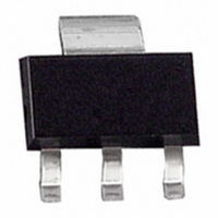
BSP317PE6327T Infineon Technologies, BSP317PE6327T Datasheet
Home Discrete Semiconductor Products MOSFETs, GaNFETs - Single BSP317PE6327T
Manufacturer Part Number
BSP317PE6327T
Description
MOSFET P-CH 250V 430MA SOT223
Manufacturer
Infineon Technologies
Specifications of BSP317PE6327T
Fet Type
MOSFET P-Channel, Metal Oxide
Fet Feature
Logic Level Gate
Rds On (max) @ Id, Vgs
4 Ohm @ 430mA, 10V
Drain To Source Voltage (vdss)
250V
Current - Continuous Drain (id) @ 25° C
430mA
Vgs(th) (max) @ Id
2V @ 370µA
Gate Charge (qg) @ Vgs
15.1nC @ 10V
Input Capacitance (ciss) @ Vds
262pF @ 25V
Power - Max
1.8W
Mounting Type
Surface Mount
Package / Case
SOT-223 (3 leads + Tab), SC-73, TO-261
Lead Free Status / RoHS Status
Lead free / RoHS Compliant
Other names
BSP317PE6327XTINTR
Feature
• P-Channel
• Enhancement mode
• Logic Level
• dv/dt rated
SIPMOS Small-Signal-Transistor
Type
BSP317P
Maximum Ratings, at T
Parameter
Continuous drain current
T
T
Pulsed drain current
T
Reverse diode dv/dt
I
Gate source voltage
Power dissipation
T
Operating and storage temperature
IEC climatic category; DIN IEC 68-1
S
Rev.1.6
A
A
A
A
Qualified according to AEC Q101
=-0.43A, V
=25°C
=70°C
=25°C
=25°C
2.0
5
DS
=-200V, di/dt=-200A/µs, T
Package
PG-SOT223
j
= 25 °C, unless otherwise specified
Tape and Reel Information
L6327: 1000 pcs/reel
jmax
=150°C
Page 1
Symbol
I
I
dv/dt
V
P
T
D
D puls
j ,
GS
tot
T
stg
Gate
pin1
BSP317P
BSP317P
Marking
Source
pin 3
-55... +150
Drain
pin 2/4
55/150/56
Product Summary
V
R
I
Value
D
-0.43
-0.34
-1.72
DS
DS(on)
±20
1.8
6
Packaging
Non dry
PG-SOT223
4
BSP317P
2008-03-27
-0.43
-250
4
1
Unit
A
kV/µs
V
W
°C
2
VPS05163
V
Ω
A
3
Related parts for BSP317PE6327T
BSP317PE6327T Summary of contents
SIPMOS Small-Signal-Transistor Feature • P-Channel • Enhancement mode • Logic Level • dv/dt rated Qualified according to AEC Q101 Type Package PG-SOT223 BSP317P Maximum Ratings Parameter Continuous drain current T =25° ...
Thermal Characteristics Parameter Characteristics Thermal resistance, junction - soldering point (Pin 4) SMD version, device on PCB: @ min. footprint cooling area Electrical Characteristics Parameter Static Characteristics Drain-source breakdown voltage V =0, I ...
Electrical Characteristics Parameter Dynamic Characteristics Transconductance Input capacitance Output capacitance Reverse transfer capacitance Turn-on delay time Rise time Turn-off delay time Fall time Gate Charge Characteristics Gate to source charge Gate to drain charge Gate charge total Gate ...
Power dissipation tot BSP 317 P 1.9 W 1.6 1.4 1.2 1 0.8 0.6 0.4 0 Safe operating area ...
Typ. output characteristic parameter =25° 1.6 10V 5V A 4.4V 3.6V 3.2V 1.2 2.8V 2.4V 2.2V 1 0.8 0.6 0.4 0 0.5 1 1.5 2 2.5 ...
Drain-source on-state resistance DS(on) j parameter : I = -0. BSP 317 P 11 Ω 98% 4 typ -60 - ...
Typ. gate charge Gate parameter -0.43 A pulsed BSP 317 P -16 V -12 - 20% -4 50 ...
Rev.2.0 Page 8 BSP317P 2008-03-27 ...
Related keywords
bsp31 bsp315p bsp315 bsp317p bsp316 bsp318s BSP317PE6327T datasheet BSP317PE6327T data sheet BSP317PE6327T pdf datasheet BSP317PE6327T component BSP317PE6327T part BSP317PE6327T distributor BSP317PE6327T RoHS BSP317PE6327T datasheet download


