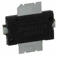
MRFE6S9045NR1 Freescale Semiconductor, MRFE6S9045NR1 Datasheet
MRFE6S9045NR1
Specifications of MRFE6S9045NR1
MRFE6S9045NR1TR
Available stocks


Related parts for MRFE6S9045NR1

MRFE6S9045NR1 Summary of contents
Page 1
... MHz AVG SINGLE N - CDMA LATERAL N - CHANNEL BROADBAND RF POWER MOSFET CASE 1265- 09, STYLE 270 - 2 PLASTIC Symbol Value Unit V - 0.5, +66 Vdc DSS Vdc GS V 32, +0 Vdc +150 °C stg T 150 ° 225 °C J (2,3) Symbol Value Unit R °C/W θJC 1.0 1.1 MRFE6S9045NR1 1 ...
Page 2
... Functional Tests (In Freescale Test Fixture, 50 ohm system CDMA, 1.2288 MHz Channel Bandwidth Carrier. ACPR measured in 30 kHz Channel Bandwidth @ ±750 kHz Offset. PAR = 9 0.01% Probability on CCDF Power Gain Drain Efficiency Adjacent Channel Power Ratio Input Return Loss MRFE6S9045NR1 2 Rating 3 = 25°C unless otherwise noted) C Symbol ...
Page 3
... Vdc 350 mA — 20 — — 68 — — — — 52 — = 350 mA, 865 - 900 MHz Bandwidth — 10 — — 0.72 — — 0.011 — — 0.006 — MRFE6S9045NR1 Unit dBc dBc MHz dB dB/°C dBm/°C 3 ...
Page 4
... Taper Z7 0.087″ x 0.525″ Microstrip Z8 0.435″ x 0.525″ Microstrip Z9 0.057″ x 0.525″ Microstrip Figure 1. MRFE6S9045NR1 Test Circuit Schematic Table 6. MRFE6S9045NR1 Test Circuit Component Designations and Values Part B1 Ferrite Bead B2 Ferrite Bead C1, C7, C10, C14 47 pF Chip Capacitors C2, C4, C12 0 ...
Page 5
... C15 Figure 2. MRFE6S9045NR1 Test Circuit Component Layout RF Device Data Freescale Semiconductor C7 C10 C11 C9 C18 V DD C16 C17 B2 C14 C13 C12 TO−270/272 Surface / Bolt down MRFE6S9045NR1 5 ...
Page 6
... Vdc 880 MHz 880.1 MHz 18 DD Two−Tone Measurements OUTPUT POWER (WATTS) PEP out Figure 5. Two - Tone Power Gain versus Output Power MRFE6S9045NR1 6 TYPICAL CHARACTERISTICS Vdc (Avg 350 mA out DQ N−CDMA IS−95 Pilot Sync, Paging Traffic Codes 8 Through 13 ALT1 820 ...
Page 7
... IM3−L IM7−U IM7−L IM5−U 10 TWO−TONE SPACING (MHz) versus Tone Spacing Ideal Actual −5 −10 25_C −15 85_C −20 25_C −25 −30 −30_C −35 −40 −30_C −45 − −30_C C −55 −60 −65 25_C −70 −75 100 MRFE6S9045NR1 100 7 ...
Page 8
... 85_C η 880 MHz OUTPUT POWER (WATTS) CW out Figure 11. Power Gain and Drain Efficiency versus CW Output Power MRFE6S9045NR1 8 TYPICAL CHARACTERISTICS 80 23 −30_C 25_C 70 85_C Vdc 19 = 350 100 Figure 12. Power Gain versus Output Power 90 110 130 150 170 190 210 T , JUNCTION TEMPERATURE (°C) ...
Page 9
... FREQUENCY (MHz) MRFE6S9045NR1 . . . . . . . . . . . . . . . . . . . . . . . . . . . . . . . . . . . . . . . . . . . . . . . . . . . . . . . . . . . . . . . . . .. . . . . . . ...
Page 10
... MHz Z source f = 850 MHz Z Z Figure 16. Series Equivalent Source and Load Impedance MRFE6S9045NR1 Ω 850 MHz Z load f = 910 MHz Vdc 350 mA Avg out source load MHz Ω Ω 850 0.42 + j0.30 3.05 + j1.27 865 0.42 + j0.44 3.16 + j1.33 880 0.45 + j0.60 3 ...
Page 11
... RF Device Data Freescale Semiconductor PACKAGE DIMENSIONS MRFE6S9045NR1 11 ...
Page 12
... MRFE6S9045NR1 12 RF Device Data Freescale Semiconductor ...
Page 13
... RF Device Data Freescale Semiconductor MRFE6S9045NR1 13 ...
Page 14
... AN3263: Bolt Down Mounting Method for High Power RF Transistors and RFICs in Over - Molded Plastic Packages Engineering Bulletins • EB212: Using Data Sheet Impedances for RF LDMOS Devices The following table summarizes revisions to this document. Revision Date 0 Oct. 2007 • Initial Release of Data Sheet MRFE6S9045NR1 14 PRODUCT DOCUMENTATION REVISION HISTORY Description RF Device Data Freescale Semiconductor ...
Page 15
... Freescale Semiconductor was negligent regarding the design or manufacture of the part. Freescalet and the Freescale logo are trademarks of Freescale Semiconductor, Inc. All other product or service names are the property of their respective owners. © Freescale Semiconductor, Inc. 2007. All rights reserved. MRFE6S9045NR1 15 ...