MRFE6S9045NR1 Freescale Semiconductor, MRFE6S9045NR1 Datasheet - Page 2
MRFE6S9045NR1
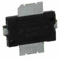
Manufacturer Part Number
MRFE6S9045NR1
Description
MOSFET RF N-CH 10W TO-270-2
Manufacturer
Freescale Semiconductor
Datasheet
1.MRFE6S9045NR1.pdf
(15 pages)
Specifications of MRFE6S9045NR1
Transistor Type
N-Channel
Frequency
880MHz
Gain
22.1dB
Voltage - Rated
66V
Current Rating
10µA
Current - Test
350mA
Voltage - Test
28V
Power - Output
10W
Package / Case
TO-270-2
Drain Source Voltage Vds
66V
Rf Transistor Case
TO-270
Termination Type
SMD
Output Power Pout
10W
Peak Reflow Compatible (260 C)
Yes
Transistor Polarity
N Channel
Rohs Compliant
Yes
Channel Type
N
Channel Mode
Enhancement
Drain Source Voltage (max)
66V
Output Power (max)
10W
Power Gain (typ)@vds
22.1/20/20dB
Frequency (max)
1GHz
Package Type
TO-270
Pin Count
3
Input Capacitance (typ)@vds
81@28VpF
Output Capacitance (typ)@vds
27@28VpF
Reverse Capacitance (typ)
1.02@28VpF
Operating Temp Range
-65C to 225C
Drain Efficiency (typ)
32%
Mounting
Surface Mount
Mode Of Operation
1-Carrier N-CDMA/CW/GSM EDGE
Number Of Elements
1
Vswr (max)
5
Screening Level
Military
Filter Terminals
SMD
Gate-source Voltage
12V
Leaded Process Compatible
Yes
Operating Frequency Max
880MHz
Lead Free Status / RoHS Status
Contains lead / RoHS Compliant
Noise Figure
-
Lead Free Status / Rohs Status
Compliant
Other names
MRFE6S9045NR1
MRFE6S9045NR1TR
MRFE6S9045NR1TR
Available stocks
Company
Part Number
Manufacturer
Quantity
Price
Company:

Part Number:
MRFE6S9045NR1
Manufacturer:
ELNA
Quantity:
4 000
Part Number:
MRFE6S9045NR1
Manufacturer:
FREESCALE
Quantity:
20 000


MRFE6S9045NR1
2
Table 3. ESD Protection Characteristics
Table 4. Moisture Sensitivity Level
Table 5. Electrical Characteristics
Off Characteristics
On Characteristics
Dynamic Characteristics
Functional Tests (In Freescale Test Fixture, 50 ohm system) V
N - CDMA, 1.2288 MHz Channel Bandwidth Carrier. ACPR measured in 30 kHz Channel Bandwidth @ ±750 kHz Offset. PAR = 9.8 dB
@ 0.01% Probability on CCDF
Human Body Model (per JESD22 - A114)
Machine Model (per EIA/JESD22 - A115)
Charge Device Model (per JESD22 - C101)
Per JESD 22 - A113, IPC/JEDEC J - STD - 020
Zero Gate Voltage Drain Leakage Current
Zero Gate Voltage Drain Leakage Current
Gate - Source Leakage Current
Gate Threshold Voltage
Gate Quiescent Voltage
Drain - Source On - Voltage
Reverse Transfer Capacitance
Output Capacitance
Input Capacitance
Power Gain
Drain Efficiency
Adjacent Channel Power Ratio
Input Return Loss
(V
(V
(V
(V
(V
(V
(V
(V
(V
DS
DS
GS
DS
DD
GS
DS
DS
DS
= 66 Vdc, V
= 28 Vdc, V
= 10 Vdc, I
= 28 Vdc ± 30 mV(rms)ac @ 1 MHz, V
= 28 Vdc ± 30 mV(rms)ac @ 1 MHz, V
= 28 Vdc, V
= 5 Vdc, V
= 28 Vdc, I
= 10 Vdc, I
DS
D
D
D
GS
GS
GS
= 200 μA)
= 350 mAdc, Measured in Functional Test)
= 1.0 Adc)
= 0 Vdc)
= 0 Vdc)
= 0 Vdc)
= 0 Vdc ± 30 mV(rms)ac @ 1 MHz)
Test Methodology
Characteristic
Test Methodology
(T
C
= 25°C unless otherwise noted)
GS
GS
= 0 Vdc)
= 0 Vdc)
DD
= 28 Vdc, I
Symbol
DQ
V
Rating
V
V
ACPR
I
I
I
C
DS(on)
C
GS(th)
GS(Q)
C
G
IRL
DSS
DSS
GSS
η
= 350 mA, P
3
oss
rss
iss
ps
D
0.05
30.5
Min
Package Peak Temperature
out
2.3
—
—
—
—
—
—
21
—
—
1
= 10 W Avg., f = 880 MHz, Single - Carrier
0.23
1.02
22.1
260
Typ
- 46
- 19
3.1
27
81
32
—
—
—
2
3A (Minimum)
IV (Minimum)
A (Minimum)
Class
Freescale Semiconductor
Max
- 44
3.8
0.3
10
10
25
—
—
—
—
- 9
1
3
RF Device Data
(continued)
μAdc
μAdc
μAdc
Unit
Unit
Vdc
Vdc
Vdc
dBc
dB
dB
°C
pF
pF
pF
%
Related parts for MRFE6S9045NR1
Image
Part Number
Description
Manufacturer
Datasheet
Request
R

Part Number:
Description:
Manufacturer:
Freescale Semiconductor, Inc
Datasheet:
Part Number:
Description:
Manufacturer:
Freescale Semiconductor, Inc
Datasheet:
Part Number:
Description:
Manufacturer:
Freescale Semiconductor, Inc
Datasheet:
Part Number:
Description:
Manufacturer:
Freescale Semiconductor, Inc
Datasheet:
Part Number:
Description:
Manufacturer:
Freescale Semiconductor, Inc
Datasheet:
Part Number:
Description:
Manufacturer:
Freescale Semiconductor, Inc
Datasheet:
Part Number:
Description:
Manufacturer:
Freescale Semiconductor, Inc
Datasheet:
Part Number:
Description:
Manufacturer:
Freescale Semiconductor, Inc
Datasheet:
Part Number:
Description:
Manufacturer:
Freescale Semiconductor, Inc
Datasheet:
Part Number:
Description:
Manufacturer:
Freescale Semiconductor, Inc
Datasheet:
Part Number:
Description:
Manufacturer:
Freescale Semiconductor, Inc
Datasheet:
Part Number:
Description:
Manufacturer:
Freescale Semiconductor, Inc
Datasheet:
Part Number:
Description:
Manufacturer:
Freescale Semiconductor, Inc
Datasheet:
Part Number:
Description:
Manufacturer:
Freescale Semiconductor, Inc
Datasheet:
Part Number:
Description:
Manufacturer:
Freescale Semiconductor, Inc
Datasheet: