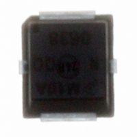
MRFG35010ANR5 Freescale Semiconductor, MRFG35010ANR5 Datasheet

MRFG35010ANR5
Specifications of MRFG35010ANR5
Available stocks
Related parts for MRFG35010ANR5
MRFG35010ANR5 Summary of contents
Page 1
... For reliable operation, the operating channel temperature should not exceed 150°C. 2. Refer to AN1955, Thermal Measurement Methodology of RF Power Amplifiers http://www.freescale.com/rf. Select Documentation/Application Notes - AN1955. © Freescale Semiconductor, Inc., 2006, 2008. All rights reserved. RF Device Data Freescale Semiconductor Document Number: MRFG35010A ...
Page 2
... Typ Max — 2.9 — — < 1 100 μAdc — 0.09 1 mAdc — mAdc - 1.2 - 0.8 - 0.7 - 1.2 - 0 Avg 3550 MHz, out 9 10 — — — 140 mA 3550 MHz — 10 — RF Device Data Freescale Semiconductor Unit Adc Vdc Vdc dB % dBc W ...
Page 3
... Chip Capacitors C3, C15 100 pF Chip Capacitors C4, C13, C14 100 pF Chip Capacitors C5, C12 1000 pF Chip Capacitors C6, C11 0.1 μF Chip Capacitors C7, C10 39K Chip Capacitors C8 μ Chip Capacitors R1 Ω Chip Resistors RF Device Data Freescale Semiconductor R2 C13 C4 C14 C3 C15 C2 C16 Z12 Z9, Z10 ...
Page 4
... Figure 2. 3.5 GHz Test Circuit Component Layout MRFG35010AR1 4 C13 C12 C11 C10 C14 C15 C16 C17 MRFG35010, Rev Device Data Freescale Semiconductor ...
Page 5
... NOTE: All data is referenced to package lead interface. Γ All data is generated from load pull, not from the test circuit shown. RF Device Data Freescale Semiconductor TYPICAL CHARACTERISTICS Vdc 140 mA 3550 MHz DS DQ Single−Carrier W−CDMA 3.84 MHz Channel Bandwidth Γ ...
Page 6
... OUTPUT POWER (dBm) out and Drain Efficiency versus Output Power = 12 Vdc 140 mA 3550 MHz DS DQ IRL ACPR OUTPUT POWER (dBm) out Figure 6. Single - Carrier W - CDMA ACPR and Input Return Loss versus Output Power −10 −15 −20 −25 − Device Data Freescale Semiconductor ...
Page 7
... Figure 7. Series Equivalent Source and Load Impedance RF Device Data Freescale Semiconductor load f = 3550 MHz Z source f = 3550 MHz Vdc 140 mA Avg out source load MHz W W 3550 4.6 - j18.7 4 Test circuit impedance as measured from source gate to ground Test circuit impedance as measured load from drain to ground ...
Page 8
... RF Device Data Freescale Semiconductor ...
Page 9
... RF Device Data Freescale Semiconductor ( Vdc 1000 mA ∠ φ 1.305 27.2 0.0250 1.296 25.8 0.0258 1.287 24.4 0.0264 1 ...
Page 10
... RF Device Data Freescale Semiconductor ...
Page 11
... RF Device Data Freescale Semiconductor ( Vdc 1000 mA ∠ φ 0.752 108.7 0.1006 0.704 105.4 0.0959 0.660 102.3 0.0915 ...
Page 12
... RF Device Data Freescale Semiconductor ...
Page 13
... RF Device Data Freescale Semiconductor ( Vdc 140 mA ∠ φ 1.151 24.7 0.0256 1.141 23.3 0.0262 1.132 21.9 ...
Page 14
... RF Device Data Freescale Semiconductor ...
Page 15
... RF Device Data Freescale Semiconductor ( Vdc 140 mA ∠ φ 0.684 105.6 0.0930 0.638 102.3 0.0882 0.598 99.2 ...
Page 16
... M .355 .365 9.02 9. .355 .365 9.96 10.16 Q .125 .135 3.18 3.43 R .225 .235 5.72 5.97 S .225 .235 5.72 5.97 aaa .005 0.13 bbb .010 0.25 ccc .015 0.38 STYLE 1: PIN 1. GATE 2. DRAIN 3. SOURCE RF Device Data Freescale Semiconductor ...
Page 17
... Removed ”Operating Case Temperature Range” from Maximum Ratings table so that the maximum channel temperature rating is the limiting thermal design criteria and not the case temperature range • Added Table 3, ESD Protection Characteristics renumbered subsequent tables RF Device Data Freescale Semiconductor PRODUCT DOCUMENTATION REVISION HISTORY Description ...
Page 18
... Freescale Semiconductor product could create a situation where personal injury or death may occur. Should Buyer ...


