SD3933 STMicroelectronics, SD3933 Datasheet
SD3933
Specifications of SD3933
SD3933
Available stocks


Related parts for SD3933


SD3933 Summary of contents
Page 1
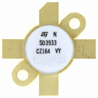
... P = 350 W min. with 29 dB gain @ 30 MHz OUT ■ In compliance with the 2002/95/EEC European directive Description The SD3933 is an N-channel MOS field-effect RF power transistor intended for use in 100 V DC large signal applications up to 200 MHz. Table 1. Device summary Part number SD3933 November 2010 HF/VHF/UHF N-channel MOSFETs Figure 1 ...
Page 2
... Electrical data . . . . . . . . . . . . . . . . . . . . . . . . . . . . . . . . . . . . . . . . . . . . . . 3 1.1 Maximum ratings . . . . . . . . . . . . . . . . . . . . . . . . . . . . . . . . . . . . . . . . . . . . 3 1.2 Thermal data . . . . . . . . . . . . . . . . . . . . . . . . . . . . . . . . . . . . . . . . . . . . . . . 3 2 Electrical characteristics . . . . . . . . . . . . . . . . . . . . . . . . . . . . . . . . . . . . . 4 2.1 Static . . . . . . . . . . . . . . . . . . . . . . . . . . . . . . . . . . . . . . . . . . . . . . . . . . . . . 4 2.2 Dynamic . . . . . . . . . . . . . . . . . . . . . . . . . . . . . . . . . . . . . . . . . . . . . . . . . . . 4 3 Impedance data . . . . . . . . . . . . . . . . . . . . . . . . . . . . . . . . . . . . . . . . . . . . . 5 4 Typical performance . . . . . . . . . . . . . . . . . . . . . . . . . . . . . . . . . . . . . . . . . 6 5 Test circuit . . . . . . . . . . . . . . . . . . . . . . . . . . . . . . . . . . . . . . . . . . . . . . . . 10 6 Circuit layout . . . . . . . . . . . . . . . . . . . . . . . . . . . . . . . . . . . . . . . . . . . . . . 13 7 VGS/GFS sorts . . . . . . . . . . . . . . . . . . . . . . . . . . . . . . . . . . . . . . . . . . . . . 14 8 Package mechanical data . . . . . . . . . . . . . . . . . . . . . . . . . . . . . . . . . . . . 17 9 Revision history . . . . . . . . . . . . . . . . . . . . . . . . . . . . . . . . . . . . . . . . . . . 18 2/19 Doc ID 9966 Rev 8 SD3933 ...
Page 3
... SD3933 1 Electrical data 1.1 Maximum ratings Table 2. Absolute maximum ratings (T Symbol (1) V Drain source voltage (BR)DSS V Drain-gate voltage (R DGR V Gate-source voltage GS I Drain current D P Power dissipation DISS T Max. operating junction temperature J T Storage temperature STG 150 °C J 1.2 Thermal data Table 3 ...
Page 4
... V = 100 MHz 100 MHz DS Test conditions I = 250 MHz 250 mA P 350 MHz DQ OUT = I = 250 350 MHz DQ OUT I = 250 mA P 300 MHz DQ OUT = Doc ID 9966 Rev 8 SD3933 Min Typ Max Unit 250 500 nA 1.5 2.5 4.0 V 2.5 3 1000 pF 265 Min Typ Max ...
Page 5
... SD3933 3 Impedance data Figure 2. Impedance data Table 6. Impedance data Freq 30 MHz Typical Input Impedance G Zin Z (Ω 2.5 Doc ID 9966 Rev 8 Impedance data Typical Drain Load Impedance S Z (Ω 7.5 5/19 ...
Page 6
... Ciss MHz 100 120 0 Figure 6. 1.6 1.4 1.2 1.0 0.8 0 +25 °C Vgs = 10 V 0.4 2.0 2.5 3.0 -50 Doc ID 9966 Rev 8 Drain current vs gate source voltage Tc = +25 °C Vds = 100 Vgs(V) Gate source voltage vs case temperature Idq = 250 mA - (°C) SD3933 5 100 ...
Page 7
... SD3933 Figure 7. Output power vs input power 500 450 400 350 300 250 200 150 100 50 0 0.0 0.1 0.2 0.3 0.4 Pin (W) Figure 9. Power gain vs output power Vdd = 100 200 300 Pout (W) Figure 8. 500 450 Vdd = 100 V 400 Vdd = 90 V 350 ...
Page 8
... Figure 14. Output power vs supply voltage 500 450 400 350 300 250 200 150 100 50 0 300 400 Doc ID 9966 Rev +85, +70, +50, +25 °C 0 100 200 300 Pout (W) Pin = 0.62 W Pin = 0. Vdd (V) SD3933 MHz Vds = 100 V Idq = 250 mA 400 500 MHz Tc = +25 °C 90 100 ...
Page 9
... SD3933 Figure 15. Output power vs gate source voltage 400 350 300 250 200 150 100 Vgs (V) Pin = 27.8 dBm Vdd = 100 +25 ° MHz Doc ID 9966 Rev 8 Typical performance 9/19 ...
Page 10
... Inductor,1 3/4 turn air-wound#16AWG BELDEN ID = 0.225 Poly-coated Magnet Wire FAIR-RITE CORP 3 turns AWG #14 wire through fair rite toroid FAIR-RITE CORP 3 turns AWG #14 wire through fair rite toroid FAIR-RITE CORP Toroid SPC TECHNOLOGY Clear teflon shrink tubing Doc ID 9966 Rev 8 SD3933 50V + - Description ...
Page 11
... SD3933 Table 7. Components part list (continued) ° Item Qty Part TYPE 8011 16 1 108-0910-001 15 1 108-0902-001 14 1 108-0903-001 545562 92196A108 9 8 91252A251 8 3 92196A146 7 4 WLS-04-017- 92196A108 5 2 5050-0037 C16 1 C15 1 C14 1 C13 1 ATC700B122MW50X C12 1 SKR470M1JF11V C11 1 ATC200B103MW50X C10 1 ATC200B103MW50X C9 1 C1812X7R501-103KNE ...
Page 12
... Test circuit Table 7. Components part list (continued) ° Item Qty Part 12/19 Vendor 180 pF ATC 100B surface mount ceramic chip ATC capacitor 750 pF ATC 700B surface mount ceramic chip ATC capacitor Doc ID 9966 Rev 8 SD3933 Description ...
Page 13
... SD3933 6 Circuit layout Figure 17. Test fixture component layout Figure 18. Test circuit photometers LOG1101 SD3933 SD2923 LOG1101 Doc ID 9966 Rev 8 Circuit layout 13/19 ...
Page 14
... Doc ID 9966 Rev 8 SD3933 Gfs(min) Gfs(max ...
Page 15
... SD3933 Table 8. VGS/GFS sorts (continued) Marking Vgs(min) Vgs(max) 2.25 2.50 2.25 2.50 2.25 2.50 2.25 2.50 2.50 2.75 2.50 2.75 2.50 2.75 2.50 2.75 2.50 2.75 2.50 2.75 2.50 2.75 2.50 2.75 2.50 2.75 2.75 3.00 2.75 3.00 2.75 3.00 2.75 3 ...
Page 16
... Doc ID 9966 Rev 8 SD3933 Gfs(min) Gfs(max ...
Page 17
... SD3933 8 Package mechanical data In order to meet environmental requirements, ST offers these devices in different grades of ® ECOPACK packages, depending on their level of environmental compliance. ECOPACK specifications, grade definitions and product status are available at: www.st.com. ® ECOPACK trademark. Table 9. M177 (.550 DIA 4/L N/HERM W/FLG) mechanical data Dim ...
Page 18
... Revision 1 First release 2 Idss value updated 3 Specification upgrade Table 8: VGS/GFS sorts on page 14 4 Added Table 4: Static on page 4 5 Updated Table 8: VGS/GFS sorts on page 14 6 Updated 7 Updated features on cover page. 8 Updated package name. Doc ID 9966 Rev 8 SD3933 Changes ...
Page 19
... SD3933 Information in this document is provided solely in connection with ST products. STMicroelectronics NV and its subsidiaries (“ST”) reserve the right to make changes, corrections, modifications or improvements, to this document, and the products and services described herein at any time, without notice. All ST products are sold pursuant to ST’s terms and conditions of sale. ...