BLF1820-90,112 NXP Semiconductors, BLF1820-90,112 Datasheet - Page 2
BLF1820-90,112
Manufacturer Part Number
BLF1820-90,112
Description
TRANSISTOR RF LDMOS SOT502A
Manufacturer
NXP Semiconductors
Datasheet
1.BLF1820-90112.pdf
(12 pages)
Specifications of BLF1820-90,112
Package / Case
SOT502A
Transistor Type
LDMOS
Frequency
2GHz
Gain
11dB
Voltage - Rated
65V
Current Rating
12A
Current - Test
750mA
Voltage - Test
26V
Power - Output
90W
Configuration
Single
Transistor Polarity
N-Channel
Resistance Drain-source Rds (on)
0.1 Ohms
Drain-source Breakdown Voltage
65 V
Gate-source Breakdown Voltage
+/- 15 V
Continuous Drain Current
12 A
Maximum Operating Temperature
+ 200 C
Mounting Style
SMD/SMT
Minimum Operating Temperature
- 65 C
Lead Free Status / RoHS Status
Lead free / RoHS Compliant
Noise Figure
-
Lead Free Status / RoHS Status
Lead free / RoHS Compliant, Lead free / RoHS Compliant
Other names
934056520112
BLF1820-90
BLF1820-90
BLF1820-90
BLF1820-90


Philips Semiconductors
FEATURES
APPLICATIONS
DESCRIPTION
90 W LDMOS power transistor for base station
applications at frequencies from 1800 to 2000 MHz.
QUICK REFERENCE DATA
RF performance at T
LIMITING VALUES
In accordance with the Absolute Maximum Rating System (IEC 60134).
2003 Feb 10
2-tone, class-AB
V
V
I
T
T
MODE OF OPERATION
This product is supplied in anti-static packing to prevent damage caused by electrostatic discharge during transport
and handling. For further information, refer to Philips specs.: SNW-EQ-608, SNW-FQ-302A and SNW-FQ-302B.
D
stg
j
Typical 2-tone performance at a supply voltage of 26 V
and I
– Output power = 90 W (PEP)
– Gain = 12 dB
– Efficiency = 32%
– dim = 26 dBc
Easy power control
Excellent ruggedness
High power gain
Excellent thermal stability
Designed for broadband operation (1800 to 2000 MHz)
Internally matched for ease of use.
RF power amplifiers for GSM, EDGE and CDMA base
stations and multicarrier applications in the
1800 to 2000 MHz frequency range.
DS
GS
UHF power LDMOS transistor
DQ
SYMBOL
of 500 mA:
h
= 25 C in a common source test circuit.
f
drain-source voltage
gate-source voltage
DC drain current
storage temperature
junction temperature
1
= 2000; f
(MHz)
2
f
= 2000.1
PARAMETER
CAUTION
V
(V)
2
26
DS
PINNING
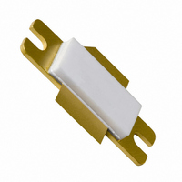
handbook, halfpage
PIN
90 (PEP)
1
2
3
(W)
P
Fig.1 Simplified outline SOT502A.
L
Top view
drain
gate
source, connected to flange
(dB)
>11
G
p
1
2
DESCRIPTION
MIN.
65
Product specification
BLF1820-90
>30
(%)
MBK394
3
D
65
12
+150
200
MAX.
15
(dBc)
d
V
V
A
UNIT
im
C
C
25
Related parts for BLF1820-90,112
Image
Part Number
Description
Manufacturer
Datasheet
Request
R

Part Number:
Description:
Uhf Power Ldmos Transistor
Manufacturer:
NXP Semiconductors
Datasheet:
Part Number:
Description:
RF MOSFET Small Signal BULK TNS-RFPR
Manufacturer:
NXP Semiconductors
Datasheet:
Part Number:
Description:
NXP Semiconductors designed the LPC2420/2460 microcontroller around a 16-bit/32-bitARM7TDMI-S CPU core with real-time debug interfaces that include both JTAG andembedded trace
Manufacturer:
NXP Semiconductors
Datasheet:

Part Number:
Description:
NXP Semiconductors designed the LPC2458 microcontroller around a 16-bit/32-bitARM7TDMI-S CPU core with real-time debug interfaces that include both JTAG andembedded trace
Manufacturer:
NXP Semiconductors
Datasheet:
Part Number:
Description:
NXP Semiconductors designed the LPC2468 microcontroller around a 16-bit/32-bitARM7TDMI-S CPU core with real-time debug interfaces that include both JTAG andembedded trace
Manufacturer:
NXP Semiconductors
Datasheet:
Part Number:
Description:
NXP Semiconductors designed the LPC2470 microcontroller, powered by theARM7TDMI-S core, to be a highly integrated microcontroller for a wide range ofapplications that require advanced communications and high quality graphic displays
Manufacturer:
NXP Semiconductors
Datasheet:
Part Number:
Description:
NXP Semiconductors designed the LPC2478 microcontroller, powered by theARM7TDMI-S core, to be a highly integrated microcontroller for a wide range ofapplications that require advanced communications and high quality graphic displays
Manufacturer:
NXP Semiconductors
Datasheet:
Part Number:
Description:
The Philips Semiconductors XA (eXtended Architecture) family of 16-bit single-chip microcontrollers is powerful enough to easily handle the requirements of high performance embedded applications, yet inexpensive enough to compete in the market for hi
Manufacturer:
NXP Semiconductors
Datasheet:
Part Number:
Description:
The XA-S3 device is a member of Philips Semiconductors? XA(eXtended Architecture) family of high performance 16-bitsingle-chip microcontrollers
Manufacturer:
NXP Semiconductors
Datasheet:

Part Number:
Description:
The NXP BlueStreak LH75401/LH75411 family consists of two low-cost 16/32-bit System-on-Chip (SoC) devices
Manufacturer:
NXP Semiconductors
Datasheet:
Part Number:
Description:
The NXP LPC3130/3131 combine an 180 MHz ARM926EJ-S CPU core, high-speed USB2
Manufacturer:
NXP Semiconductors
Datasheet:
Part Number:
Description:
The NXP LPC3141 combine a 270 MHz ARM926EJ-S CPU core, High-speed USB 2
Manufacturer:
NXP Semiconductors
Part Number:
Description:
The NXP LPC3143 combine a 270 MHz ARM926EJ-S CPU core, High-speed USB 2
Manufacturer:
NXP Semiconductors

Part Number:
Description:
The NXP LPC3152 combines an 180 MHz ARM926EJ-S CPU core, High-speed USB 2
Manufacturer:
NXP Semiconductors