2STBN15D100 STMicroelectronics, 2STBN15D100 Datasheet
2STBN15D100
Specifications of 2STBN15D100


Related parts for 2STBN15D100


2STBN15D100 Summary of contents
Page 1
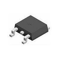
... Darlington configuration. Table 1. Device summary Order code 2STBN15D100T4 January 2010 Low voltage NPN power Darlington transistor Figure kΩ 150 Ω Marking Package BN15D100 D²PAK Doc ID 16117 Rev 2 2STBN15D100 TAB 3 1 D²PAK Internal schematic diagrams Packaging Tape and reel www.st.com 1/7 7 ...
Page 2
... Total dissipation at T TOT T Storage temperature STG T Max. operating junction temperature J Table 3. Thermal data Symbol R Thermal resistance junction-case max. thJC 2/7 Parameter = °C case Parameter Doc ID 16117 Rev 2 2STBN15D100 Value Unit 100 V 100 0 -65 to 150 °C 150 °C Value Unit 1.8 °C/W ...
Page 3
... Electrical characteristics °C; unless otherwise specified. case Table 4. Electrical characteristics Symbol Collector cut-off current I CBO ( Collector cut-off current I CEO ( Emitter cut-off current I EBO ( Collector-emitter (1) V CEO(sus) sustaining voltage (I Collector-emitter (1) V CE(sat) saturation voltage (1) V Base-emitter on voltage BE(on) ( current gain FE V Diode forward voltage F 1. Pulse test: pulse duration ≤ ...
Page 4
... Package mechanical data 3 Package mechanical data In order to meet environmental requirements, ST offers these devices in different grades of ® ECOPACK packages, depending on their level of environmental compliance. ECOPACK specifications, grade definitions and product status are available at: www.st.com. ® ECOPACK trademark. 4/7 Doc ID 16117 Rev 2 2STBN15D100 ® ...
Page 5
... Dim D²PAK (TO-263) mechanical data mm Min Typ Max 4.40 4.60 0.03 0.23 0.70 0.93 1.14 1.70 0.45 0.60 1.23 1.36 8.95 9.35 7.50 10 10.40 8.50 2.54 4.88 5.28 15 15.85 2.49 2.69 2.29 2.79 1.27 1.40 1.30 1.75 0.4 0° 8° ...
Page 6
... Revision history 4 Revision history Table 5. Document revision history Date 01-Sep-2009 19-Jan-2010 6/7 Revision 1 First release. 2 Modified Table 1 on page Doc ID 16117 Rev 2 2STBN15D100 Changes 1. ...
Page 7
... Information in this document is provided solely in connection with ST products. STMicroelectronics NV and its subsidiaries (“ST”) reserve the right to make changes, corrections, modifications or improvements, to this document, and the products and services described herein at any time, without notice. All ST products are sold pursuant to ST’s terms and conditions of sale. ...