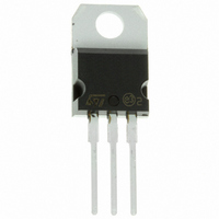
BD244C STMicroelectronics, BD244C Datasheet

BD244C
Specifications of BD244C
BD244CST
BD244CST
Available stocks
Related parts for BD244C
BD244C Summary of contents
Page 1
... Power linear and switching Description The device is manufactured in Planar technology with “Base Island” layout. The resulting transistor shows exceptional high gain performance coupled with very low saturation voltage. The PNP type is BD244C. Table 1. Device summary Order code BD243C BD244C July 2007 Complementary power transistors ...
Page 2
... B P Total dissipation at T TOT T Storage temperature stg T Max. operating junction temperature J Note: For PNP types voltage and current values are negative 2/10 Parameter BD243C (NPN < 5ms 25°C c BD243C BD244C Value Unit BD244C (PNP) 100 V 100 -65 to 150 °C 150 °C ...
Page 3
... BD243C BD244C 2 Electrical characteristics (T = 25°C; unless otherwise specified) case Table 3. Electrical characteristics Symbol Collector cut-off current I CES (V BE Collector cut-off current I CEO ( Emitter cut-off current I EBO ( Collector-emitter (1) V CEO(sus) sustaining voltage (I Collector-emitter (1) V CE(sat) saturation voltage (1) V Base-emitter voltage BE (1) ...
Page 4
... Electrical characteristics 2.1 Typical characteristics Figure 2. Safe operating area Figure 4. DC current gain (NPN) Figure 6. Collector-emitter saturation voltage (NPN) 4/10 BD243C BD244C Figure 3. Derating curve Figure 5. DC current gain (PNP) Figure 7. Collector-emitter saturation voltage (PNP) ...
Page 5
... BD243C BD244C Figure 8. Base-emitter saturation voltage (NPN) Figure 10. Base-emitter saturation voltage (NPN) Figure 12. BT(ON) time (NPN) Electrical characteristics Figure 9. Base-emitter saturation voltage (PNP) Figure 11. Base-emitter saturation voltage (PNP) Figure 13. BT time (PNP) (ON) 5/10 ...
Page 6
... Figure 14. Resistive load switching time (NPN) Figure 16. Resistive load switching time (NPN) Figure 18. Collector-base and collector- emitter capacitance (NPN) 6/10 BD243C BD244C Figure 15. Resistive load switching time (PNP) Figure 17. Resistive load switching time (PNP) Figure 19. Collector-base and collector- emitter capacitance (PNP) ...
Page 7
... BD243C BD244C 3 Package mechanical data In order to meet environmental requirements, ST offers these devices in ECOPACK® packages. These packages have a Lead-free second level interconnect . The category of second level interconnect is marked on the package and on the inner box label, in compliance with JEDEC Standard JESD97. The maximum ratings related to soldering conditions are also marked on the inner box label ...
Page 8
... L30 øP Q 8/10 TO-220 Mechanical data mm. MIN. TYP 4.40 0.61 1.14 0.49 15.25 1.27 10 2.40 4.95 1.23 6.20 2.40 13 3.50 16.40 28.90 3.75 2.65 BD243C BD244C MAX. 4.60 0.88 1.70 0.70 15.75 10.40 2.70 5.15 1.32 6.60 2.72 14 3.93 3.85 2.95 ...
Page 9
... BD243C BD244C 4 Revision history Table 4. Revision history Date 13-Sep-2005 25-Jul-2007 Revision 4 New datasheet according to MLD-PWR/05/1267 Figures 10, 11, 12, 13, 14, 15, 16, 17, 18 and 5 figure 19, added Revision history Changes 9/10 ...
Page 10
... Australia - Belgium - Brazil - Canada - China - Czech Republic - Finland - France - Germany - Hong Kong - India - Israel - Italy - Japan - Malaysia - Malta - Morocco - Singapore - Spain - Sweden - Switzerland - United Kingdom - United States of America 10/10 Please Read Carefully: © 2007 STMicroelectronics - All rights reserved STMicroelectronics group of companies www.st.com BD243C BD244C ...


