BU941P STMicroelectronics, BU941P Datasheet
BU941P
Specifications of BU941P
BU941P
Available stocks


Related parts for BU941P


BU941P Summary of contents
Page 1
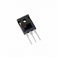
... Order codes BU941 BU941P November 2008 High voltage ignition coil driver NPN power Darlington transistors 1 2 TO-3 Figure 1. for TO-3 Marking Package BU941 TO-3 BU941P TO-247 Rev 3 BU941 BU941P 1 TO-247 Internal schematic diagrams for TO-247 Packaging Tray Tube www.st.com 3 2 1/12 12 ...
Page 2
... Content Content 1 Electrical ratings . . . . . . . . . . . . . . . . . . . . . . . . . . . . . . . . . . . . . . . . . . . . 3 2 Electrical characteristics . . . . . . . . . . . . . . . . . . . . . . . . . . . . . . . . . . . . . 4 2.1 Electrical characteristics (curves Test circuits . . . . . . . . . . . . . . . . . . . . . . . . . . . . . . . . . . . . . . . . . . . . . . . . 7 4 Package mechanical data . . . . . . . . . . . . . . . . . . . . . . . . . . . . . . . . . . . . . 8 5 Revision history . . . . . . . . . . . . . . . . . . . . . . . . . . . . . . . . . . . . . . . . . . . 11 2/12 BU941, BU941P ...
Page 3
... BU941, BU941P 1 Electrical ratings Table 2. Absolute maximum ratings Symbol V Collector-emitter voltage (V CES V Collector-emitter voltage (I CEO V Emitter-base voltage (I EBO I Collector current C I Collector peak current CM I Base current B I Base peak current BM P Total dissipation at T TOT T Storage temperature stg T Max. operating junction temperature J Table 3 ...
Page 4
... 400 V clamp = 0) B Figure 12 see 400 V clamp Figure 9 see BU941, BU941P Min. Typ. Max. 100 T = 125 °C 0.5 C 100 T = 125 °C 0 400 I = 100 mA 1 250 mA 1 300 100 mA 2 250 mA 2 300 mA 2 300 CE 2 300 V clamp Ω 0.5 Figure 11 see Unit µ ...
Page 5
... BU941, BU941P 2.1 Electrical characteristics (curves) Figure 2. Safe operating area Figure 4. DC current gain Figure 6. Collector-emitter saturation voltage Figure 7. Electrical characteristics Figure 3. DC current gain Figure 5. Collector-emitter saturation voltage Base-emitter saturation voltage 5/12 ...
Page 6
... Electrical characteristics Figure 8. Switching time inductive load 6/12 BU941, BU941P ...
Page 7
... BU941, BU941P 3 Test circuits Figure 9. Functional test circuit Figure 11. Switching time test circuit Figure 10. Functional test wafeforms Figure 12. Sustaining voltage test circuit Test circuits 7/12 ...
Page 8
... These packages have a lead-free second level interconnect . The category of second level interconnect is marked on the package and on the inner box label, in compliance with JEDEC Standard JESD97. The maximum ratings related to soldering conditions are also marked on the inner box label. ECOPACK trademark. ECOPACK specifications are available at: www.st.com 8/12 BU941, BU941P ...
Page 9
... BU941, BU941P DIM TO-3 mechanical data mm. min. typ 11.00 0.9 7 1.50 8.32 19.00 10.70 16.50 25.00 4.00 38.50 30.00 Package mechanical data max. 13.10 1 .15 1.65 8.92 20.00 11.10 17.20 26.00 4.09 39.30 30.30 0015923C 9/12 ...
Page 10
... Package mechanical data Dim øP øR S 10/12 TO-247 Mechanical data mm. Min. Typ 4.85 2.20 1.0 2.0 3.0 0.40 19.85 15.45 5.45 14.20 3.70 18.50 3.55 4.50 5.50 BU941, BU941P Max. 5.15 2.60 1.40 2.40 3.40 0.80 20.15 15.75 14.80 4.30 3.65 5.50 ...
Page 11
... BU941, BU941P 5 Revision history Table 5. Document revision history Date 21-Jun-2004 18-Nov-2008 Revision 2 3 Package changed from TO-218 to TO-247 for BU941P. Revision history Changes 11/12 ...
Page 12
... Australia - Belgium - Brazil - Canada - China - Czech Republic - Finland - France - Germany - Hong Kong - India - Israel - Italy - Japan - Malaysia - Malta - Morocco - Singapore - Spain - Sweden - Switzerland - United Kingdom - United States of America 12/12 Please Read Carefully: © 2008 STMicroelectronics - All rights reserved STMicroelectronics group of companies www.st.com BU941, BU941P ...