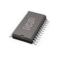
TDA9887T/V4 NXP Semiconductors, TDA9887T/V4 Datasheet - Page 11

TDA9887T/V4
Manufacturer Part Number
TDA9887T/V4
Description
RF Receiver DEMODULATOR VIF AND SIF
Manufacturer
NXP Semiconductors
Type
Transmitter/Receiverr
Datasheet
1.TDA9887TV4.pdf
(58 pages)
Specifications of TDA9887T/V4
Package / Case
SO-24
Operating Frequency
58.75 MHz
Operating Supply Voltage
5 V
Maximum Operating Temperature
+ 70 C
Minimum Operating Temperature
- 20 C
Mounting Style
SMD/SMT
Operating Temperature (min)
-20C
Operating Temperature (max)
70C
Operating Temperature Classification
Commercial
Operating Supply Voltage (min)
4.5V
Operating Supply Voltage (typ)
5V
Operating Supply Voltage (max)
5.5V
Lead Free Status / RoHS Status
Lead free / RoHS Compliant
Other names
TDA9887T/V4,112
Available stocks
Company
Part Number
Manufacturer
Quantity
Price
Part Number:
TDA9887T/V4
Manufacturer:
PHILIPS/飞利浦
Quantity:
20 000
Philips Semiconductors
8.5
The VCO of the VIF-FPLL operates as an integrated low
radiation relaxation oscillator at double the picture carrier
frequency. The control voltage, required to tune the VCO
to double the picture carrier frequency, is generated at the
loop filter by the frequency phase detector. The possible
frequency range is 50 to 140 MHz (typical value).
The oscillator frequency is divided-by-two to provide two
differential square wave signals with exactly 90 degrees
phase difference, independent of the frequency, for use in
the FPLL detectors, the video demodulator and the
intercarrier mixer.
8.6
Each relaxation oscillator of the VIF-PLL and FM-PLL
demodulator has a wide frequency range. To prevent false
locking of the PLLs and with respect to the catching range,
the digital acquisition help provides an individual control,
until the frequency of the VCO is within the preselected
standard dependent lock-in window of the PLL.
The in-window and out-window control at the FM-PLL is
additionally used to mute the audio stage (if auto mute is
selected via the I
The working principle of the digital acquisition help is as
follows. The PLL VCO output is connected to a down
counter which has a predefined start value (standard
dependent). The VCO frequency clocks the down counter
for a fixed gate time. Thereafter, the down counter stop
value is analysed. In case the stop value is higher (lower)
than the expected value range, the VCO frequency is
lower (higher) than the wanted lock-in window frequency
range. A positive (negative) control current is injected into
the PLL loop filter and consequently the VCO frequency is
increased (decreased) and a new counting cycle starts.
The gate time as well as the control logic of the acquisition
help circuit is dependent on the precision of the reference
signal at pin REF. Operation as a crystal oscillator is
possible as well as connecting this input via a serial
capacitor to an external reference frequency, e.g. the
tuning system oscillator.
The AFC signal is derived from the corresponding down
counter stop value after a counting cycle. The last four bits
are latched and can be read out via the I
(see Table 7). Also the digital-to-analog converted value is
given as current at pin AFC.
2004 Aug 25
I
IF-PLL demodulator with FM radio
2
C-bus controlled multistandard alignment-free
VCO and divider
AFC and digital acquisition help
2
C-bus).
2
C-bus
11
8.7
The video demodulator is realized by a multiplier which is
designed for low distortion and large bandwidth. The VIF
signal is multiplied with the ‘in phase’ signal of the VIF-PLL
VCO.
The demodulator output signal is fed into the video
preamplifier via a level shift stage with integrated low-pass
filter to achieve carrier harmonics attenuation.
The output signal of the preamplifier is fed to the VIF-AGC
detector (see Section 8.3) and in the sound trap mode also
fed internally to the integrated sound carrier trap
(see Section 8.8). The differential trap output signal is
converted and amplified by the following postamplifier.
The video output level at pin CVBS is 2 V (p-p).
In the bypass mode the output signal of the preamplifier is
fed directly through the postamplifier to pin CVBS. The
output video level is 1.1 V (p-p) for using an external sound
trap with 10 % overall loss.
Noise clipping is provided in both cases.
8.8
The sound carrier trap consists of a reference filter, a
phase detector and the sound trap itself.
A sound carrier reference signal is fed into the reference
low-pass filter and is shifted by nominal 90 degrees. The
phase detector compares the original reference signal with
the signal shifted by the reference filter and produces a
DC voltage by charging or discharging an integrated
capacitor with a current proportional to the phase
difference between both signals, respectively to the
frequency error of the integrated filters. The DC voltage
controls the frequency position of the reference filter and
the sound trap. So the accurate frequency position for the
different standards is set by the sound carrier reference
signal.
The sound trap itself is constructed of three separate traps
to realize sufficient suppression of the first and second
sound carriers.
8.9
The SIF amplifier consists of three AC-coupled differential
stages. Gain control is performed by emitter degeneration.
The total gain control range is typically 66 dB. The
differential input impedance is typically 2 k in parallel with
3 pF.
Video demodulator and amplifier
Sound carrier trap
SIF amplifier
Product specification
TDA9887


