PBSS3540E,115 NXP Semiconductors, PBSS3540E,115 Datasheet
PBSS3540E,115
Specifications of PBSS3540E,115
PBSS3540E T/R
PBSS3540E T/R


Related parts for PBSS3540E,115


PBSS3540E,115 Summary of contents
Page 1
PBSS3540E 40 V, 500 mA PNP low V Rev. 02 — 11 December 2009 1. Product profile 1.1 General description PNP low V plastic package. NPN complement: PBSS2540E. 1.2 Features Low collector-emitter saturation voltage V High collector current capability: I ...
Page 2
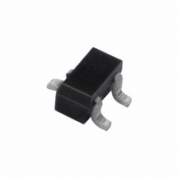
... NXP Semiconductors 2. Pinning information Table 2. Pin Ordering information Table 3. Type number PBSS3540E 4. Marking Table 4. Type number PBSS3540E PBSS3540E_2 Product data sheet 40 V, 500 mA PNP low V Pinning Description base emitter collector Ordering information Package Name Description SC-75 plastic surface mounted package; 3 leads ...
Page 3
... NXP Semiconductors 5. Limiting values Table 5. In accordance with the Absolute Maximum Rating System (IEC 60134). Symbol V CBO V CEO V EBO tot amb T stg [1] Device mounted on an FR4 PCB, single-sided copper, tin-plated and standard footprint. [2] Device mounted on an FR4 PCB, single-sided copper, tin-plated, mounting pad for collector 1 cm ...
Page 4
... NXP Semiconductors 6. Thermal characteristics Table 6. Symbol R th(j-a) [1] Device mounted on an FR4 PCB, single-sided copper, tin-plated and standard footprint. [2] Device mounted on an FR4 PCB, single-sided copper, tin-plated, mounting pad for collector duty cycle = 1 Z th(j-a) 0.75 (K/W) 0.5 0. 0.2 0.1 0.05 0. ...
Page 5
... NXP Semiconductors 7. Characteristics Table 7. Characteristics ° unless otherwise specified. amb Symbol Parameter I collector-base cut-off CBO current I emitter-base cut-off EBO current h DC current gain FE V collector-emitter CEsat saturation voltage R collector-emitter CEsat saturation resistance V base-emitter BEsat saturation voltage V base-emitter turn-on BEon voltage f transition frequency ...
Page 6
... NXP Semiconductors 600 ( 400 (2) (3) 200 0 −1 −10 −1 −10 = − 100 °C (1) T amb = 25 °C (2) T amb = −55 °C (3) T amb Fig 3. DC current gain as a function of collector current; typical values −1 V CEsat (V) −1 −10 (1) (2) (3) −2 −10 −1 −10 − ...
Page 7
... NXP Semiconductors −1.1 V BEsat (V) −0.9 (1) (2) −0.7 (3) −0.5 −0.3 −0.1 −1 −10 −1 − −55 °C (1) T amb = 25 °C (2) T amb = 100 °C (3) T amb Fig 7. Base-emitter saturation voltage as a function of collector current; typical values −1 (mA) = − −27 C (A) −24 −21 − ...
Page 8
... NXP Semiconductors 8. Package outline Fig 11. Package outline SOT416 (SC-75) 9. Packing information Table 8. Packing methods The indicated -xxx are the last three digits of the 12NC ordering code. Type number Package Description PBSS3540E SOT416 4 mm pitch tape and reel [1] For further information and the availability of packing methods, see 10 ...
Page 9
... Document ID Release date PBSS3540E_2 20091211 • Modifications: This data sheet was changed to reflect the new company name NXP Semiconductors, including new legal definitions and disclaimers. No changes were made to the technical content. • Figure 4 “Base-emitter voltage as a function of collector current; typical • ...
Page 10
... Right to make changes — NXP Semiconductors reserves the right to make changes to information published in this document, including without limitation specifications and product descriptions, at any time and without notice ...
Page 11
... NXP Semiconductors 14. Contents 1 Product profile . . . . . . . . . . . . . . . . . . . . . . . . . . 1 1.1 General description . . . . . . . . . . . . . . . . . . . . . 1 1.2 Features . . . . . . . . . . . . . . . . . . . . . . . . . . . . . . 1 1.3 Applications . . . . . . . . . . . . . . . . . . . . . . . . . . . 1 1.4 Quick reference data . . . . . . . . . . . . . . . . . . . . 1 2 Pinning information . . . . . . . . . . . . . . . . . . . . . . 2 3 Ordering information . . . . . . . . . . . . . . . . . . . . . 2 4 Marking . . . . . . . . . . . . . . . . . . . . . . . . . . . . . . . . 2 5 Limiting values Thermal characteristics . . . . . . . . . . . . . . . . . . 4 7 Characteristics . . . . . . . . . . . . . . . . . . . . . . . . . . 5 8 Package outline . . . . . . . . . . . . . . . . . . . . . . . . . 8 9 Packing information . . . . . . . . . . . . . . . . . . . . . 8 10 Soldering . . . . . . . . . . . . . . . . . . . . . . . . . . . . . . 8 11 Revision history . . . . . . . . . . . . . . . . . . . . . . . . . 9 12 Legal information ...