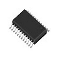
LMX2354TM National Semiconductor, LMX2354TM Datasheet

LMX2354TM
Specifications of LMX2354TM
Available stocks
Related parts for LMX2354TM
LMX2354TM Summary of contents
Page 1
... LMX2354 (2.5 GHz) — 7.0 mA. The LMX2354 are available in a 24-pin TSSOP surface mount plastic package and 24-pin CSP. Functional Block Diagram © 2001 National Semiconductor Corporation Features n Pin compatible/functional equivalent to the LMX2350 n Enhanced Low Noise Fractional Engine n 2 ...
Page 2
... Connection Diagrams www.national.com 20004802 Order Number LMX2354TM or LMX2355TM See NS Package Number MTC24 20004822 Order Number LMX2354SLB or LMX2355SLB See NS Package Number SLB 2 ...
Page 3
Pin Descriptions Pin No. for Pin No. for Pin TSSOP CSP Name Package Package 1 24 OUT0 GND 6 5 fin RF 7 ...
Page 4
Absolute Maximum Ratings Parameter Power Supply Voltage Voltage on any pin with GND = 0V Storage Temperature Range Lead Temperature (Solder 4 sec.) Recommended Operating Conditions Parameter Power Supply Voltage Operating Temperature Note 1: “Absolute Maximum Ratings” indicate limits beyond ...
Page 5
Electrical Characteristics All min/max specifications are guaranteed by design, or test, or statistical methods. (Continued) Symbol Parameter ICPo- IF Charge Pump Output source IF Current (see Programming ICPo- sink IF Description 3.1.4) ICPo- source IF ICPo- sink IF ICPo- Charge ...
Page 6
Charge Pump Current Specification Definitions sink current − sink current Vp sink current ...
Page 7
RF Sensitivity Test Block Diagram Note 10,000 Note: Sensitivity limit is reached when the error of the divided RF output, F Typical Performance Characteristics LMX2354 Charge Pump ...
Page 8
Typical Performance Characteristics Sink vs Source Mismatch (See (Note 6) under Charge Pump Current Specification Definitions) IF Input Impedance V = 2.7V to 5.5V 550 MHz (f Capacitor = 100 pF) IN www.national.com (Continued) 20004830 = 50 ...
Page 9
Typical Performance Characteristics IF Input Sensitivity vs Frequency (Continued) Oscillator Input Sensitivity vs Frequency 20004835 9 20004836 www.national.com ...
Page 10
... GENERAL The basic phase-lock-loop (PLL) configuration consists of a high-stability crystal reference oscillator, a frequency synthe- sizer such as the National Semiconductor LMX2354, a volt- age controlled oscillator (VCO), and a passive loop filter. The frequency synthesizer includes a phase detector, current mode charge pump, as well as programmable reference [R] and feedback [N] frequency dividers ...
Page 11
Functional Description LMX2354 RF N Counter Register in Fractional Mode with P = 8/9/12/ 1–23 Divide ratios less than 24 are impossible since it is required that C 3 24–39 Some of these values ...
Page 12
Functional Description 1.8 Fo/LD MULTIFUNCTION OUTPUT The Fo/LD output pin can deliver several internal functions including analog/digital lock detects, and counter outputs. See programming description 4.1.5 for more details. 1.8.1 Lock Detect A digital filtered lock detect function is included ...
Page 13
Programming Description 3.0 INPUT DATA REGISTER The descriptions below describe the 24-bit data register loaded through the MICROWIRE Interface. The data register is used to program the 15-bit IF_R counter register, and the 15-bit RF_R counter register, the 15-bit IF_N ...
Page 14
Programming Description 4.1.3 15-BIT PROGRAMMABLE REFERENCE DIVIDER RATIO (R COUNTER) Divide Ratio • • • • • 32,767 Notes: Divide ratio: 3 ...
Page 15
Programming Description 4.2.1 (RF_R[22]–RF_R[23]) DLL_MODE BIT LOCATION DLL_MODE RF_R [23] V2_EN RF_R [22] Note 1. V2_EN bit when set high enables the voltage doubler for the RF Charge Pump supply. Note 2. DLL_MODE bit should be set to one for ...
Page 16
Programming Description 5.1.2 CMOS (Programmable CMOS outputs) MSB FastLock Note: Test bit is reserved and should be set to zero for normal usage. 5.1.3 Programmable CMOS Output Truth Table Bit Location OUT_0 IF_N[17] OUT_1 IF_N[18] Test IF_N[19] Fastlock IF_N[20] Test ...
Page 17
Programming Description 5.2 RF_N Register If the control bits (CTL[2:0]) are 1 1, data is transferred from the 24-bit shift register into the RF_N register latch which sets the RF PLL’s programmable N counter register and various control functions. The ...
Page 18
Programming Description 5.2.2 N REGISTER — (8/9/12/13) PRESCALER OPERATING IN FRACTIONAL MODE Divide Ratio 1–23 Divide Ratios Less than 24 are impossible since it is required that C 24– ... . . ...
Page 19
Programming Description 5.3 QUADRATURE MODULUS PRESCALER The LMX2354 contains a quadrature modulus prescaler, consisting of a prescaler, A counter, B counter and C counter. Once the N value is known, the A, B, and C values can be calculated by: ...
Page 20
Programming Description 5.5 LOCK DETECT DIGITAL FILTER The Lock Detect Digital Filter compares the difference between the phase of the inputs of the phase detector generated delay of approximately 15 ns. To enter the locked state (Lock ...
Page 21
Programming Description 5.6 ANALOG LOCK DETECT FILTER When the Fo/LD output is configured in analog lock detect mode an external lock detect circuit is needed in order to provide a steady LOW signal when the PLL is in the locked ...
Page 22
... Physical Dimensions www.national.com inches (millimeters) unless otherwise noted Thin Shrink Small Outline (TSSOP) Package Order Number LMX2354TM For Tape and Reel (2500 Units per Reel) Order Number LMX2354TMX NS Package Number MTC24 22 ...
Page 23
... NATIONAL’S PRODUCTS ARE NOT AUTHORIZED FOR USE AS CRITICAL COMPONENTS IN LIFE SUPPORT DEVICES OR SYSTEMS WITHOUT THE EXPRESS WRITTEN APPROVAL OF THE PRESIDENT AND GENERAL COUNSEL OF NATIONAL SEMICONDUCTOR CORPORATION. As used herein: 1. Life support devices or systems are devices or systems which, (a) are intended for surgical implant ...


