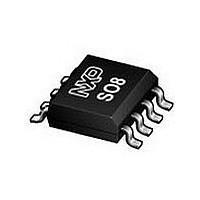
ICM7555CD NXP Semiconductors, ICM7555CD Datasheet - Page 13

ICM7555CD
Manufacturer Part Number
ICM7555CD
Description
Manufacturer
NXP Semiconductors
Type
Standardr
Datasheet
1.ICM7555CD.pdf
(22 pages)
Specifications of ICM7555CD
# Internal Timers
1
Power Dissipation
780mW
Operating Supply Voltage (min)
3V
Operating Supply Voltage (typ)
3.3/5/9/12/15V
Operating Supply Voltage (max)
16V
Package Type
SO
High Level Output Current
-1mA
Low Level Output Current
3.2mA
Pin Count
8
Operating Temp Range
0C to 70C
Operating Temperature Classification
Commercial
Mounting
Surface Mount
Lead Free Status / RoHS Status
Compliant
Available stocks
Company
Part Number
Manufacturer
Quantity
Price
Company:
Part Number:
ICM7555CD
Manufacturer:
NXP
Quantity:
1 945
Part Number:
ICM7555CD
Manufacturer:
NXP/恩智浦
Quantity:
20 000
Part Number:
ICM7555CD/01
Manufacturer:
NXP/恩智浦
Quantity:
20 000
Company:
Part Number:
ICM7555CD/01,118
Manufacturer:
Intel
Quantity:
52
Company:
Part Number:
ICM7555CD/01118
Manufacturer:
NXP Semiconductors
Quantity:
269 796
NXP Semiconductors
ICM7555_2
Product data sheet
11.6 Control voltage
11.7 RESET
The CONTROL_VOLTAGE terminal permits the two trip voltages for the THRESHOLD
and TRIGGER internal comparators to be controlled. This provides the possibility of
oscillation frequency modulation in the astable mode, or even inhibition of oscillation,
depending on the applied voltage. In the monostable mode, delay times can be changed
by varying the applied voltage to the CONTROL_VOLTAGE pin.
The RESET terminal is designed to have essentially the same trip voltage as the standard
NE/SE555 device, i.e., 0.6 V to 0.7 V. At all supply voltages it represents an extremely
high input impedance. The mode of operation of the RESET function is, however, much
improved over the standard NE/SE555 device in that it controls only the internal flip-flop,
which in turn controls simultaneously the state of the OUTPUT and DISCHARGE pins.
This avoids the multiple threshold problems sometimes encountered with slow falling
edges in the NE/SE555 devices.
Fig 16. Monostable operation
V
DD
18 V; t = 1.05 R
Rev. 02 — 3 August 2009
A
1
2
3
4
C
GND
TRIGGER
OUTPUT
RESET
CONTROL_VOLTAGE
THRESHOLD
DISCHARGE
V
DD
8
7
6
5
V
General purpose CMOS timer
DD
optional
capacitor
R A
002aae419
© NXP B.V. 2009. All rights reserved.
ICM7555
C
13 of 22


