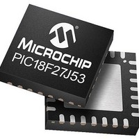
PIC16LF1903-E/MV Microchip Technology, PIC16LF1903-E/MV Datasheet - Page 73

PIC16LF1903-E/MV
Manufacturer Part Number
PIC16LF1903-E/MV
Description
7KB Flash, 256B RAM, LCD, 11x10b ADC, NanoWatt XLP 28 UQFN 4x4x0.5mm TUBE
Manufacturer
Microchip Technology
Series
PIC® XLP™ 16Fr
Datasheet
1.PIC16LF1902-EMV.pdf
(240 pages)
Specifications of PIC16LF1903-E/MV
Processor Series
PIC16LF190x
Core
PIC
Data Bus Width
8 bit
Program Memory Type
Flash
Program Memory Size
4 KB
Data Ram Size
256 B
Maximum Clock Frequency
20 MHz
Number Of Programmable I/os
25
Number Of Timers
2
Operating Supply Voltage
1.8 V to 3.6 V
Maximum Operating Temperature
+ 125 C
Mounting Style
SMD/SMT
Package / Case
QFN-28
Core Processor
PIC
Core Size
8-Bit
Speed
20MHz
Connectivity
-
Peripherals
Brown-out Detect/Reset, LCD, POR, PWM, WDT
Number Of I /o
25
Eeprom Size
-
Ram Size
256 x 8
Voltage - Supply (vcc/vdd)
1.8 V ~ 3.6 V
Data Converters
A/D 11x10b
Oscillator Type
Internal
Operating Temperature
-40°C ~ 125°C
Lead Free Status / Rohs Status
Details
- Current page: 73 of 240
- Download datasheet (3Mb)
8.0
The Power-Down mode is entered by executing a
SLEEP instruction.
Upon entering Sleep mode, the following conditions
exist:
1.
2.
3.
4.
5.
6.
7.
8.
9.
10. Resets other than WDT are not affected by
Refer to individual chapters for more details on
peripheral operation during Sleep.
To minimize current consumption, the following condi-
tions should be considered:
• I/O pins should not be floating
• External circuitry sinking current from I/O pins
• Internal circuitry sourcing current from I/O pins
• Current draw from pins with internal weak pull-ups
• Modules using 31 kHz LFINTOSC
• Modules using Secondary oscillator
I/O pins that are high-impedance inputs should be
pulled to V
rents caused by floating inputs.
Examples of internal circuitry that might be sourcing
current include the FVR module. See
age Reference (FVR)”
2011 Microchip Technology Inc.
WDT will be cleared but keeps running, if
enabled for operation during Sleep.
PD bit of the STATUS register is cleared.
TO bit of the STATUS register is set.
CPU clock is disabled.
31 kHz LFINTOSC is unaffected and peripherals
that operate from it may continue operation in
Sleep.
Secondary oscillator is unaffected and peripher-
als that operate from it may continue operation
in Sleep.
ADC is unaffected, if the dedicated FRC clock is
selected.
Capacitive Sensing oscillator is unaffected.
I/O ports maintain the status they had before
SLEEP was executed (driving high, low or
high-impedance).
Sleep mode.
POWER-DOWN MODE (SLEEP)
DD
or V
SS
externally to avoid switching cur-
for more information.
13.0 “Fixed Volt-
Preliminary
8.1
The device can wake-up from Sleep through one of the
following events:
1.
2.
3.
4.
5.
6.
The first three events will cause a device Reset. The
last three events are considered a continuation of pro-
gram execution. To determine whether a device Reset
or wake-up event occurred, refer to
Determining the Cause of a
When the SLEEP instruction is being executed, the next
instruction (PC + 1) is prefetched. For the device to
wake-up through an interrupt event, the corresponding
interrupt enable bit must be enabled. Wake-up will
occur regardless of the state of the GIE bit. If the GIE
bit is disabled, the device continues execution at the
instruction after the SLEEP instruction. If the GIE bit is
enabled, the device executes the instruction after the
SLEEP instruction, the device will then call the Interrupt
Service Routine. In cases where the execution of the
instruction following SLEEP is not desirable, the user
should have a NOP after the SLEEP instruction.
The WDT is cleared when the device wakes up from
Sleep, regardless of the source of wake-up.
External Reset input on MCLR pin, if enabled
BOR Reset, if enabled
POR Reset
Watchdog Timer, if enabled
Any external interrupt
Interrupts by peripherals capable of running dur-
ing Sleep (see individual peripheral for more
information)
Wake-up from Sleep
PIC16LF1902/3
Reset.
DS41455B-page 73
Section 5.11,
Related parts for PIC16LF1903-E/MV
Image
Part Number
Description
Manufacturer
Datasheet
Request
R

Part Number:
Description:
IC, 8BIT MCU, PIC16LF, 32MHZ, QFN-28
Manufacturer:
Microchip Technology
Datasheet:

Part Number:
Description:
IC, 8BIT MCU, PIC16LF, 32MHZ, QFN-28
Manufacturer:
Microchip Technology
Datasheet:

Part Number:
Description:
IC, 8BIT MCU, PIC16LF, 32MHZ, DIP-18
Manufacturer:
Microchip Technology
Datasheet:

Part Number:
Description:
IC, 8BIT MCU, PIC16LF, 20MHZ, TQFP-44
Manufacturer:
Microchip Technology
Datasheet:

Part Number:
Description:
7 KB Flash, 384 Bytes RAM, 32 MHz Int. Osc, 16 I/0, Enhanced Mid Range Core, Nan
Manufacturer:
Microchip Technology

Part Number:
Description:
14KB Flash, 512B RAM, LCD, 11x10b ADC, EUSART, NanoWatt XLP 28 SOIC .300in T/R
Manufacturer:
Microchip Technology
Datasheet:

Part Number:
Description:
14KB Flash, 512B RAM, LCD, 11x10b ADC, EUSART, NanoWatt XLP 28 SSOP .209in T/R
Manufacturer:
Microchip Technology
Datasheet:

Part Number:
Description:
MCU PIC 14KB FLASH XLP 28-SSOP
Manufacturer:
Microchip Technology

Part Number:
Description:
MCU PIC 14KB FLASH XLP 28-SOIC
Manufacturer:
Microchip Technology

Part Number:
Description:
MCU PIC 512B FLASH XLP 28-UQFN
Manufacturer:
Microchip Technology

Part Number:
Description:
MCU PIC 14KB FLASH XLP 28-SPDIP
Manufacturer:
Microchip Technology

Part Number:
Description:
MCU 7KB FLASH 256B RAM 40-UQFN
Manufacturer:
Microchip Technology

Part Number:
Description:
MCU 7KB FLASH 256B RAM 44-TQFP
Manufacturer:
Microchip Technology

Part Number:
Description:
MCU 14KB FLASH 1KB RAM 28-UQFN
Manufacturer:
Microchip Technology

Part Number:
Description:
MCU PIC 14KB FLASH XLP 40-UQFN
Manufacturer:
Microchip Technology


