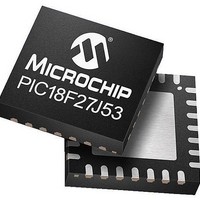
PIC16LF1903-E/MV Microchip Technology, PIC16LF1903-E/MV Datasheet - Page 95

PIC16LF1903-E/MV
Manufacturer Part Number
PIC16LF1903-E/MV
Description
7KB Flash, 256B RAM, LCD, 11x10b ADC, NanoWatt XLP 28 UQFN 4x4x0.5mm TUBE
Manufacturer
Microchip Technology
Series
PIC® XLP™ 16Fr
Datasheet
1.PIC16LF1902-EMV.pdf
(240 pages)
Specifications of PIC16LF1903-E/MV
Processor Series
PIC16LF190x
Core
PIC
Data Bus Width
8 bit
Program Memory Type
Flash
Program Memory Size
4 KB
Data Ram Size
256 B
Maximum Clock Frequency
20 MHz
Number Of Programmable I/os
25
Number Of Timers
2
Operating Supply Voltage
1.8 V to 3.6 V
Maximum Operating Temperature
+ 125 C
Mounting Style
SMD/SMT
Package / Case
QFN-28
Core Processor
PIC
Core Size
8-Bit
Speed
20MHz
Connectivity
-
Peripherals
Brown-out Detect/Reset, LCD, POR, PWM, WDT
Number Of I /o
25
Eeprom Size
-
Ram Size
256 x 8
Voltage - Supply (vcc/vdd)
1.8 V ~ 3.6 V
Data Converters
A/D 11x10b
Oscillator Type
Internal
Operating Temperature
-40°C ~ 125°C
Lead Free Status / Rohs Status
Details
- Current page: 95 of 240
- Download datasheet (3Mb)
11.0
In general, when a peripheral is enabled on a port pin,
that pin cannot be used as a general purpose output.
However, the pin can still be read.
Each port has three standard registers for its operation.
These registers are:
• TRISx registers (data direction)
• PORTx registers (reads the levels on the pins of
• LATx registers (output latch)
Some ports may have one or more of the following
additional registers. These registers are:
• ANSELx (analog select)
• WPUx (weak pull-up)
TABLE 11-1:
The Data Latch (LATA register) is useful for
read-modify-write operations on the value that the I/O
pins are driving.
A write operation to the LATA register has the same
effect as a write to the corresponding PORTA register.
A read of the LATA register reads of the values held in
the I/O PORT latches, while a read of the PORTA
register reads the actual I/O pin value.
Ports that support analog inputs have an associated
ANSELx register. When an ANSEL bit is set, the digital
input buffer associated with that bit is disabled.
Disabling the input buffer prevents analog signal levels
on the pin between a logic high and low from causing
excessive current in the logic input circuitry. A
simplified model of a generic I/O port, without the
interfaces to other peripherals, is shown in
2011 Microchip Technology Inc.
Device
PIC16LF1902/3
the device)
I/O PORTS
PORT AVAILABILITY PER
DEVICE
●
●
●
Figure
●
11-1.
Preliminary
FIGURE 11-1:
EXAMPLE 11-1:
; This code example illustrates
; initializing the PORTA register. The
; other ports are initialized in the same
; manner.
BANKSEL PORTA
CLRF
BANKSEL LATA
CLRF
BANKSEL ANSELA
CLRF
BANKSEL TRISA
MOVLW
MOVWF
To peripherals
Write PORTx
Write LATx
Data Bus
Read PORTx
PORTA
LATA
ANSELA
B'00111000' ;Set RA<5:3> as inputs
TRISA
Data Register
PIC16LF1902/3
D
CK
Read LATx
ANSELx
GENERIC I/O PORT
OPERATION
INITIALIZING PORTA
Q
;
;Init PORTA
;Data Latch
;
;
;digital I/O
;
;and set RA<2:0> as
;outputs
TRISx
DS41455B-page 95
V
V
DD
SS
I/O pin
Related parts for PIC16LF1903-E/MV
Image
Part Number
Description
Manufacturer
Datasheet
Request
R

Part Number:
Description:
IC, 8BIT MCU, PIC16LF, 32MHZ, QFN-28
Manufacturer:
Microchip Technology
Datasheet:

Part Number:
Description:
IC, 8BIT MCU, PIC16LF, 32MHZ, QFN-28
Manufacturer:
Microchip Technology
Datasheet:

Part Number:
Description:
IC, 8BIT MCU, PIC16LF, 32MHZ, DIP-18
Manufacturer:
Microchip Technology
Datasheet:

Part Number:
Description:
IC, 8BIT MCU, PIC16LF, 20MHZ, TQFP-44
Manufacturer:
Microchip Technology
Datasheet:

Part Number:
Description:
7 KB Flash, 384 Bytes RAM, 32 MHz Int. Osc, 16 I/0, Enhanced Mid Range Core, Nan
Manufacturer:
Microchip Technology

Part Number:
Description:
14KB Flash, 512B RAM, LCD, 11x10b ADC, EUSART, NanoWatt XLP 28 SOIC .300in T/R
Manufacturer:
Microchip Technology
Datasheet:

Part Number:
Description:
14KB Flash, 512B RAM, LCD, 11x10b ADC, EUSART, NanoWatt XLP 28 SSOP .209in T/R
Manufacturer:
Microchip Technology
Datasheet:

Part Number:
Description:
MCU PIC 14KB FLASH XLP 28-SSOP
Manufacturer:
Microchip Technology

Part Number:
Description:
MCU PIC 14KB FLASH XLP 28-SOIC
Manufacturer:
Microchip Technology

Part Number:
Description:
MCU PIC 512B FLASH XLP 28-UQFN
Manufacturer:
Microchip Technology

Part Number:
Description:
MCU PIC 14KB FLASH XLP 28-SPDIP
Manufacturer:
Microchip Technology

Part Number:
Description:
MCU 7KB FLASH 256B RAM 40-UQFN
Manufacturer:
Microchip Technology

Part Number:
Description:
MCU 7KB FLASH 256B RAM 44-TQFP
Manufacturer:
Microchip Technology

Part Number:
Description:
MCU 14KB FLASH 1KB RAM 28-UQFN
Manufacturer:
Microchip Technology

Part Number:
Description:
MCU PIC 14KB FLASH XLP 40-UQFN
Manufacturer:
Microchip Technology


