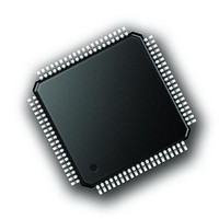
PIC18F87K90T-I/PT Microchip Technology, PIC18F87K90T-I/PT Datasheet - Page 381

PIC18F87K90T-I/PT
Manufacturer Part Number
PIC18F87K90T-I/PT
Description
128kB Flash, 4kB RAM, 1kB EE, 16MIPS, NanoWatt XLP, LCD, 5V 80 TQFP 12x12x1mm T/
Manufacturer
Microchip Technology
Series
PIC® XLP™ 18Fr
Datasheet
1.PIC18F66K90-IMR.pdf
(570 pages)
Specifications of PIC18F87K90T-I/PT
Processor Series
PIC18F
Core
PIC
Data Bus Width
8 bit
Program Memory Type
Flash
Program Memory Size
128 KB
Data Ram Size
4 KB
Interface Type
I2C, SPI
Maximum Clock Frequency
64 MHz
Number Of Timers
11
Operating Supply Voltage
1.8 V to 5.5 V
Maximum Operating Temperature
+ 125 C
3rd Party Development Tools
52715-96, 52716-328, 52717-734, 52712-325, EWPIC18
Minimum Operating Temperature
- 40 C
On-chip Adc
12 bit, 24 Channel
Core Processor
PIC
Core Size
8-Bit
Speed
64MHz
Connectivity
I²C, LIN, SPI, UART/USART
Peripherals
Brown-out Detect/Reset, LCD, POR, PWM, WDT
Number Of I /o
69
Eeprom Size
1K x 8
Ram Size
4K x 8
Voltage - Supply (vcc/vdd)
1.8 V ~ 5.5 V
Data Converters
A/D 24x12b
Oscillator Type
Internal
Operating Temperature
-40°C ~ 85°C
Package / Case
80-TQFP
Lead Free Status / Rohs Status
Details
Available stocks
Company
Part Number
Manufacturer
Quantity
Price
Company:
Part Number:
PIC18F87K90T-I/PT
Manufacturer:
Microchip Technology
Quantity:
10 000
Company:
Part Number:
PIC18F87K90T-I/PTRSL
Manufacturer:
Microchip Technology
Quantity:
10 000
- Current page: 381 of 570
- Download datasheet (5Mb)
REGISTER 23-10: ANCON2: A/D PORT CONFIGURATION REGISTER 2
The analog reference voltage is software-selectable to
either the device’s positive and negative supply voltage
(AV
RA3/AN3/V
two additional internal voltage reference selections:
2.048V and 4.096V.
The A/D Converter can uniquely operate while the
device is in Sleep mode. To operate in Sleep, the A/D
conversion clock must be derived from the A/D
Converter’s internal RC oscillator.
The output of the Sample-and-Hold (S/H) is the input
into the converter, which generates the result via
successive approximation.
2009-2011 Microchip Technology Inc.
bit 7
Legend:
R = Readable bit
-n = Value at POR
bit 7-0
Note 1:
ANSEL23
DD
R/W-1
and AV
(1)
REF
AN12 through AN15, and AN20 to AN23, are implemented only on 80-pin devices. For 64-pin devices, the
corresponding ANSELx bits are still implemented for these channels, but have no effect.
+ and RA2/AN2/V
ANSEL<23:16>: Analog Port Configuration bits (AN23 through AN16)
0 = Pin configured as a digital port
1 = Pin configured as an analog channel — digital input disabled and any inputs read as ‘ 0 ’
ANSEL22
SS
R/W-1
) or the voltage level on the
(1)
W = Writable bit
‘1’ = Bit is set
ANSEL21
REF
R/W-1
- pins. V
(1)
REF
ANSEL20
R/W-1
+ has
(1)
U = Unimplemented bit, read as ‘0’
‘0’ = Bit is cleared
PIC18F87K90 FAMILY
ANSEL19
R/W-1
Each port pin associated with the A/D Converter can be
configured as an analog input or a digital I/O. The
ADRESH and ADRESL registers contain the result of
the A/D conversion. When the A/D conversion is com-
plete, the result is loaded into the ADRESH:ADRESL
register pair, the GO/DONE bit (ADCON0<1>) is
cleared and the A/D Interrupt Flag bit, ADIF (PIR1<6>),
is set.
A device Reset forces all registers to their Reset state.
This forces the A/D module to be turned off and any
conversion in progress is aborted. The value in the
ADRESH:ADRESL register pair is not modified for a
Power-on Reset. These registers will contain unknown
data after a Power-on Reset.
The block diagram of the A/D module is shown in
Figure
23-4.
ANSEL18
R/W-1
x = Bit is unknown
ANSEL17
R/W-1
DS39957D-page 381
ANSEL16
R/W-1
bit 0
Related parts for PIC18F87K90T-I/PT
Image
Part Number
Description
Manufacturer
Datasheet
Request
R

Part Number:
Description:
Manufacturer:
Microchip Technology Inc.
Datasheet:

Part Number:
Description:
Manufacturer:
Microchip Technology Inc.
Datasheet:

Part Number:
Description:
Manufacturer:
Microchip Technology Inc.
Datasheet:

Part Number:
Description:
Manufacturer:
Microchip Technology Inc.
Datasheet:

Part Number:
Description:
Manufacturer:
Microchip Technology Inc.
Datasheet:

Part Number:
Description:
Manufacturer:
Microchip Technology Inc.
Datasheet:

Part Number:
Description:
Manufacturer:
Microchip Technology Inc.
Datasheet:

Part Number:
Description:
Manufacturer:
Microchip Technology Inc.
Datasheet:


