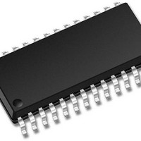
PIC24FJ16MC102-I/SO Microchip Technology, PIC24FJ16MC102-I/SO Datasheet - Page 107

PIC24FJ16MC102-I/SO
Manufacturer Part Number
PIC24FJ16MC102-I/SO
Description
16-bit Motor Control Family, 16 MIPS, 16KB Flash, 1KB RAM 28 SOIC .300in TUBE
Manufacturer
Microchip Technology
Series
PIC® 24Fr
Datasheet
1.PIC24FJ16MC101-IP.pdf
(304 pages)
Specifications of PIC24FJ16MC102-I/SO
Processor Series
PIC24FJ
Core
PIC
Data Bus Width
16 bit
Program Memory Type
Flash
Program Memory Size
16 KB
Data Ram Size
1 KB
Maximum Operating Temperature
+ 85 C
Mounting Style
SMD/SMT
Package / Case
SOIC-28
Development Tools By Supplier
MPLAB IDE Software
Minimum Operating Temperature
- 40 C
Featured Product
PIC24FJ/33FJ MCUs & dsPIC® DSCs
Core Processor
PIC
Core Size
16-Bit
Speed
16 MIPs
Connectivity
I²C, IrDA, LIN, SPI, UART/USART
Peripherals
Brown-out Detect/Reset, Motor Control PWM, POR, PWM, WDT
Number Of I /o
21
Eeprom Size
-
Ram Size
1K x 8
Voltage - Supply (vcc/vdd)
3 V ~ 3.6 V
Data Converters
A/D 6x10b
Oscillator Type
Internal
Operating Temperature
-40°C ~ 85°C
Lead Free Status / Rohs Status
Details
- Current page: 107 of 304
- Download datasheet (5Mb)
10.0
All of the device pins (except V
OSC1/CLKI) are shared among the peripherals and the
parallel I/O ports. All I/O input ports feature Schmitt
Trigger inputs for improved noise immunity.
10.1
Generally a parallel I/O port that shares a pin with a
peripheral is subservient to the peripheral. The
peripheral’s output buffer data and control signals are
FIGURE 10-1:
© 2011 Microchip Technology Inc.
Note 1: This data sheet summarizes the features
Peripheral Module
2: It
3: Some registers and associated bits
I/O PORTS
Parallel I/O (PIO) Ports
of the PIC24FJ16MC101/102 family of
devices. It is not intended to be a
comprehensive reference source. To
complement the information in this data
sheet, refer to Section 12. “I/O Ports
with Peripheral Pin Select (PPS)”
(DS39711)
Reference Manual”, which is available
from
(www.microchip.com).
specifications in
cal Characteristics”
supercede any specifications that may be
provided in PIC24F Family Reference
Manual sections.
described in this section may not be
available on all devices. Refer to
Section 4.0 “Memory Organization”
this data sheet for device-specific register
and bit information.
is
Read Port
Read LAT
Read TRIS
Data Bus
WR TRIS
WR LAT +
WR Port
important
the
BLOCK DIAGRAM OF A TYPICAL SHARED PORT STRUCTURE
Peripheral Output Enable
Peripheral Output Data
Peripheral Input Data
Peripheral Module Enable
in
Microchip
PIO Module
the
Section 26.0 “Electri-
to
DD
TRIS Latch
Data Latch
of this data sheet,
D
D
CK
CK
, V
“PIC24F
note
SS
Q
Q
, MCLR, and
web
that
Family
site
the
Preliminary
in
Output Multiplexers
provided to a pair of multiplexers. The multiplexers
select whether the peripheral or the associated port
has ownership of the output data and control signals of
the I/O pin. The logic also prevents “loop through,” in
which a port’s digital output can drive the input of a
peripheral that shares the same pin.
how ports are shared with other peripherals and the
associated I/O pin to which they are connected.
When a peripheral is enabled and the peripheral is
actively driving an associated pin, the use of the pin as
a general purpose output pin is disabled. The I/O pin
can be read, but the output driver for the parallel port bit
is disabled. If a peripheral is enabled, but the peripheral
is not actively driving a pin, that pin can be driven by a
port.
All port pins have three registers directly associated
with their operation as digital I/O. The data direction
register (TRISx) determines whether the pin is an input
or an output. If the data direction bit is a ‘1’, the pin is
an input. All port pins are defined as inputs after a
Reset. Reads from the latch (LATx) read the latch.
Writes to the latch write the latch. Reads from the port
(PORTx) read the port pins, while writes to the port pins
write the latch.
Any bit and its associated data and control registers
that are not valid for a particular device will be
disabled. This means the corresponding LATx and
TRISx registers and the port pin will read as zeros.
When a pin is shared with another peripheral or
function that is defined as an input only, it is
nevertheless regarded as a dedicated port because
there is no other competing source of outputs.
1
0
1
0
Output Enable
Output Data
PIC24FJ16MC101/102
Input Data
I/O
I/O Pin
DS39997B-page 107
Figure 10-1
shows
Related parts for PIC24FJ16MC102-I/SO
Image
Part Number
Description
Manufacturer
Datasheet
Request
R

Part Number:
Description:
Manufacturer:
Microchip Technology Inc.
Datasheet:

Part Number:
Description:
Manufacturer:
Microchip Technology Inc.
Datasheet:

Part Number:
Description:
Manufacturer:
Microchip Technology Inc.
Datasheet:

Part Number:
Description:
Manufacturer:
Microchip Technology Inc.
Datasheet:

Part Number:
Description:
Manufacturer:
Microchip Technology Inc.
Datasheet:

Part Number:
Description:
Manufacturer:
Microchip Technology Inc.
Datasheet:

Part Number:
Description:
Manufacturer:
Microchip Technology Inc.
Datasheet:

Part Number:
Description:
Manufacturer:
Microchip Technology Inc.
Datasheet:


