PIC24FJ16MC102-I/SO Microchip Technology, PIC24FJ16MC102-I/SO Datasheet - Page 298
PIC24FJ16MC102-I/SO
Manufacturer Part Number
PIC24FJ16MC102-I/SO
Description
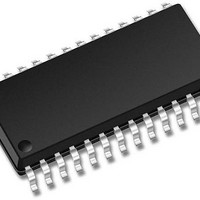
16-bit Motor Control Family, 16 MIPS, 16KB Flash, 1KB RAM 28 SOIC .300in TUBE
Manufacturer
Microchip Technology
Series
PIC® 24Fr
Datasheet
1.PIC24FJ16MC101-IP.pdf
(304 pages)
Specifications of PIC24FJ16MC102-I/SO
Processor Series
PIC24FJ
Core
PIC
Data Bus Width
16 bit
Program Memory Type
Flash
Program Memory Size
16 KB
Data Ram Size
1 KB
Maximum Operating Temperature
+ 85 C
Mounting Style
SMD/SMT
Package / Case
SOIC-28
Development Tools By Supplier
MPLAB IDE Software
Minimum Operating Temperature
- 40 C
Featured Product
PIC24FJ/33FJ MCUs & dsPIC® DSCs
Core Processor
PIC
Core Size
16-Bit
Speed
16 MIPs
Connectivity
I²C, IrDA, LIN, SPI, UART/USART
Peripherals
Brown-out Detect/Reset, Motor Control PWM, POR, PWM, WDT
Number Of I /o
21
Eeprom Size
-
Ram Size
1K x 8
Voltage - Supply (vcc/vdd)
3 V ~ 3.6 V
Data Converters
A/D 6x10b
Oscillator Type
Internal
Operating Temperature
-40°C ~ 85°C
Lead Free Status / Rohs Status
Details


PIC24FJ16MC101/102
Instruction-Based Power-Saving Modes ........................... 101
Internal RC Oscillator
Internet Address................................................................ 301
Interrupt Control and Status Registers................................ 66
Interrupt Setup Procedures ................................................. 91
Interrupt Vector Table (IVT) ................................................ 63
Interrupts Coincident with Power Save Instructions.......... 102
M
Memory Organization.......................................................... 27
Microchip Internet Web Site .............................................. 301
Motor Control PWM........................................................... 137
Motor Control PWM Module
MPLAB ASM30 Assembler, Linker, Librarian ................... 232
MPLAB Integrated Development Environment Software .. 231
MPLAB PM3 Device Programmer..................................... 234
MPLAB REAL ICE In-Circuit Emulator System................. 233
MPLINK Object Linker/MPLIB Object Librarian ................ 232
Multi-Bit Data Shifter ........................................................... 26
N
NVM Module
O
Open-Drain Configuration ................................................. 108
Output Compare................................................................ 133
P
Packaging ......................................................................... 277
PAD Configuration
Peripheral Module Disable (PMD)..................................... 102
Pinout I/O Descriptions (table) ............................................ 13
PMD Module
PORTA
PORTB
Power-on Reset (POR) ....................................................... 59
Power-Saving Features..................................................... 101
Program Address Space ..................................................... 27
DS39997B-page 298
Overview ................................................................... 226
Summary................................................................... 223
Idle ............................................................................ 102
Sleep ......................................................................... 101
Use with WDT ........................................................... 221
IECx ............................................................................ 66
IFSx............................................................................. 66
INTCON1 .................................................................... 66
INTCON2 .................................................................... 66
IPCx ............................................................................ 66
Initialization ................................................................. 91
Interrupt Disable.......................................................... 91
Interrupt Service Routine ............................................ 91
Trap Service Routine .................................................. 91
6-Output Register Map................................................ 35
Register Map............................................................... 43
Details ....................................................................... 279
Marking ............................................................. 277, 278
Register Map............................................................... 39
Register Map............................................................... 43
Register Map............................................................... 42
Register Map for PIC24FJ16MC101 ........................... 42
Register Map for PIC24FJ16MC102 ........................... 42
Clock Frequency and Switching................................ 101
Construction ................................................................ 46
Data Access from Program Memory Using
Data Access from Program Memory Using
Program Space Visibility ..................................... 49
Preliminary
Program Memory
PWM Time Base............................................................... 141
R
Reader Response............................................................. 302
Register Map
Register Maps
Registers
Data Access from, Address Generation ..................... 47
Memory Map............................................................... 27
Table Read Instructions
Visibility Operation ...................................................... 49
Interrupt Vector ........................................................... 28
Organization ............................................................... 28
Reset Vector ............................................................... 28
Real-Time Clock and Calendar................................... 39
Comparator................................................................. 40
AD1CHS123 (ADC1 Input Channel 1, 2, 3 Select)... 181
ADxCHS0 (ADCx Input Channel 0 Select ................ 182
ADxCON1 (ADCx Control 1)..................................... 177
ADxCON2 (ADCx Control 2)..................................... 179
ADxCON3 (ADCx Control 3)..................................... 180
ADxCSSL (ADCx Input Scan Select Low) ................ 183
ADxPCFGL (ADCx Port Configuration Low)............. 184
CLKDIV (Clock Divisor) .............................................. 98
CMSTAT (Comparator Status) ................................. 189
CMxCON (Comparator Control) ............................... 190
CMxFLTR (Comparator Filter Control) ..................... 196
CMxMSKCON (Comparator Mask Gating Control) .. 194
CMxMSKSRC (Comparator Mask Source Control) .. 192
CORCON (Core Control) ...................................... 25, 67
CTMUCON (CTMU Control) ............................. 211, 212
CTMUCON1 (CTMU Control Register 1).................. 211
CTMUCON1 (CTMU Control Register 2).................. 212
CTMUICON (CTMU Current Control) ....................... 213
CVRCON (Comparator Voltage Reference Control) 197
DEVID (Device ID).................................................... 219
DEVREV (Device Revision)...................................... 219
I2CxCON (I2Cx Control) ........................................... 161
I2CxMSK (I2Cx Slave Mode Address Mask) ............ 165
I2CxSTAT (I2Cx Status) ........................................... 163
IEC0 (Interrupt Enable Control 0) ............................... 75
IEC1 (Interrupt Enable Control 1) ............................... 77
IEC2 (Interrupt Enable Control 2) ............................... 78
IEC3 (Interrupt Enable Control 3) ............................... 78
IEC4 (Interrupt Enable Control 4) ............................... 79
IFS0 (Interrupt Flag Status 0) ..................................... 70
IFS1 (Interrupt Flag Status 1) ..................................... 72
IFS2 (Interrupt Flag Status 2) ..................................... 73
IFS3 (Interrupt Flag Status 3) ..................................... 73
IFS4 (Interrupt Flag Status 4) ..................................... 74
INTCON1 (Interrupt Control 1).................................... 68
INTCON2 (Interrupt Control 2).................................... 69
INTTREG Interrupt Control and Status Register ........ 90
IPC0 (Interrupt Priority Control 0) ............................... 80
IPC1 (Interrupt Priority Control 1) ............................... 81
IPC14 (Interrupt Priority Control 14) ........................... 86
IPC15 (Interrupt Priority Control 15) ........................... 87
IPC16 (Interrupt Priority Control 16) ........................... 88
IPC19 (Interrupt Priority Control 19) ........................... 89
IPC2 (Interrupt Priority Control 2) ............................... 82
IPC3 (Interrupt Priority Control 3) ............................... 83
IPC4 (Interrupt Priority Control 4) ............................... 84
Table Instructions ............................................... 48
TBLRDH ............................................................. 48
TBLRDL.............................................................. 48
© 2011 Microchip Technology Inc.
Related parts for PIC24FJ16MC102-I/SO
Image
Part Number
Description
Manufacturer
Datasheet
Request
R

Part Number:
Description:
Manufacturer:
Microchip Technology Inc.
Datasheet:
Part Number:
Description:
Manufacturer:
Microchip Technology Inc.
Datasheet:
Part Number:
Description:
Manufacturer:
Microchip Technology Inc.
Datasheet:
Part Number:
Description:
Manufacturer:
Microchip Technology Inc.
Datasheet:
Part Number:
Description:
Manufacturer:
Microchip Technology Inc.
Datasheet:
Part Number:
Description:
Manufacturer:
Microchip Technology Inc.
Datasheet:
Part Number:
Description:
Manufacturer:
Microchip Technology Inc.
Datasheet:
Part Number:
Description:
Manufacturer:
Microchip Technology Inc.
Datasheet: