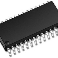
PIC24FJ16MC102-I/SO Microchip Technology, PIC24FJ16MC102-I/SO Datasheet - Page 173

PIC24FJ16MC102-I/SO
Manufacturer Part Number
PIC24FJ16MC102-I/SO
Description
16-bit Motor Control Family, 16 MIPS, 16KB Flash, 1KB RAM 28 SOIC .300in TUBE
Manufacturer
Microchip Technology
Series
PIC® 24Fr
Datasheet
1.PIC24FJ16MC101-IP.pdf
(304 pages)
Specifications of PIC24FJ16MC102-I/SO
Processor Series
PIC24FJ
Core
PIC
Data Bus Width
16 bit
Program Memory Type
Flash
Program Memory Size
16 KB
Data Ram Size
1 KB
Maximum Operating Temperature
+ 85 C
Mounting Style
SMD/SMT
Package / Case
SOIC-28
Development Tools By Supplier
MPLAB IDE Software
Minimum Operating Temperature
- 40 C
Featured Product
PIC24FJ/33FJ MCUs & dsPIC® DSCs
Core Processor
PIC
Core Size
16-Bit
Speed
16 MIPs
Connectivity
I²C, IrDA, LIN, SPI, UART/USART
Peripherals
Brown-out Detect/Reset, Motor Control PWM, POR, PWM, WDT
Number Of I /o
21
Eeprom Size
-
Ram Size
1K x 8
Voltage - Supply (vcc/vdd)
3 V ~ 3.6 V
Data Converters
A/D 6x10b
Oscillator Type
Internal
Operating Temperature
-40°C ~ 85°C
Lead Free Status / Rohs Status
Details
- Current page: 173 of 304
- Download datasheet (5Mb)
19.0
The PIC24FJ16MC101/102 devices have up to six
ADC module input channels.
19.1
The 10-bit ADC configuration has the following key
features:
• Successive Approximation (SAR) conversion
• Conversion speeds of up to 1.1 Msps
• Up to six analog input pins
• Four Sample and Hold circuits for simultaneous
• Automatic Channel Scan mode
• Selectable conversion trigger source
• Selectable Buffer Fill modes
• Four result alignment options (signed/unsigned,
• Operation during CPU Sleep and Idle modes
• 16-word conversion result buffer
Depending on the particular device pinout, the ADC
can have up to six analog input pins, designated AN0
through AN5.
Block diagrams of the ADC module are shown in
Figure 19-1
© 2011 Microchip Technology Inc.
sampling of up to four analog input pins
fractional/integer)
Note 1: This data sheet summarizes the features
2: It
3: Some registers and associated bits
10-BIT ANALOG-TO-DIGITAL
CONVERTER (ADC)
Key Features
and
of the PIC24FJ16MC101/102 family of
devices. It is not intended to be a compre-
hensive reference source. To comple-
ment the information in this data sheet,
refer to Section 46. “10-bit Analog-to-
Digital Converter (ADC) with 4 Simul-
taneous Conversions” (DS39737) in
the “PIC24F Family Reference Manual”,
which is available from the Microchip web
site (www.microchip.com).
specifications in
cal Characteristics”
supercede any specifications that may be
provided in PIC24F Family Reference
Manual sections.
described in this section may not be
available on all devices. Refer to
Section 4.0 “Memory Organization”
this data sheet for device-specific register
and bit information.
is
Figure
important
19-2.
Section 26.0 “Electri-
to
of this data sheet,
note
that
the
Preliminary
in
19.2
To configure the ADC module:
1.
2.
3.
4.
5.
6.
7.
8.
Select
(ADxPCFGH<15:0> or ADxPCFGL<15:0>).
Select voltage reference source to match
expected
(ADxCON2<15:13>).
Select the analog conversion clock to match the
desired data rate with the processor clock
(ADxCON3<7:0>).
Determine how many sample-and-hold chan-
nels
ADxPCFGH<15:0> or ADxPCFGL<15:0>).
Select
sequence
ADxCON3<12:8>).
Select the way conversion results are presented
in the buffer (ADxCON1<9:8>).
Turn on the ADC module (ADxCON1<15>).
Configure ADC interrupt (if required):
a)
b)
PIC24FJ16MC101/102
ADC Initialization
Clear the ADxIF bit.
Select the ADC interrupt priority.
will
the
port
be
range
appropriate
used
pins
(ADxCON1<7:5>
on
(ADxCON2<9:8>
as
sample/conversion
analog
DS39997B-page 173
analog
inputs
inputs
and
and
Related parts for PIC24FJ16MC102-I/SO
Image
Part Number
Description
Manufacturer
Datasheet
Request
R

Part Number:
Description:
Manufacturer:
Microchip Technology Inc.
Datasheet:

Part Number:
Description:
Manufacturer:
Microchip Technology Inc.
Datasheet:

Part Number:
Description:
Manufacturer:
Microchip Technology Inc.
Datasheet:

Part Number:
Description:
Manufacturer:
Microchip Technology Inc.
Datasheet:

Part Number:
Description:
Manufacturer:
Microchip Technology Inc.
Datasheet:

Part Number:
Description:
Manufacturer:
Microchip Technology Inc.
Datasheet:

Part Number:
Description:
Manufacturer:
Microchip Technology Inc.
Datasheet:

Part Number:
Description:
Manufacturer:
Microchip Technology Inc.
Datasheet:


