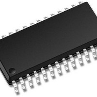
PIC24FJ16MC102-I/SO Microchip Technology, PIC24FJ16MC102-I/SO Datasheet - Page 211

PIC24FJ16MC102-I/SO
Manufacturer Part Number
PIC24FJ16MC102-I/SO
Description
16-bit Motor Control Family, 16 MIPS, 16KB Flash, 1KB RAM 28 SOIC .300in TUBE
Manufacturer
Microchip Technology
Series
PIC® 24Fr
Datasheet
1.PIC24FJ16MC101-IP.pdf
(304 pages)
Specifications of PIC24FJ16MC102-I/SO
Processor Series
PIC24FJ
Core
PIC
Data Bus Width
16 bit
Program Memory Type
Flash
Program Memory Size
16 KB
Data Ram Size
1 KB
Maximum Operating Temperature
+ 85 C
Mounting Style
SMD/SMT
Package / Case
SOIC-28
Development Tools By Supplier
MPLAB IDE Software
Minimum Operating Temperature
- 40 C
Featured Product
PIC24FJ/33FJ MCUs & dsPIC® DSCs
Core Processor
PIC
Core Size
16-Bit
Speed
16 MIPs
Connectivity
I²C, IrDA, LIN, SPI, UART/USART
Peripherals
Brown-out Detect/Reset, Motor Control PWM, POR, PWM, WDT
Number Of I /o
21
Eeprom Size
-
Ram Size
1K x 8
Voltage - Supply (vcc/vdd)
3 V ~ 3.6 V
Data Converters
A/D 6x10b
Oscillator Type
Internal
Operating Temperature
-40°C ~ 85°C
Lead Free Status / Rohs Status
Details
- Current page: 211 of 304
- Download datasheet (5Mb)
REGISTER 22-1:
© 2011 Microchip Technology Inc.
bit 15
bit 7
Legend:
R = Readable bit
-n = Value at POR
bit 15
bit 14
bit 13
bit 12
bit 11
bit 10
bit 9
bit 8
bit 7-0
Note 1:
CTMUEN
R/W-0
U-0
—
2:
If TGEN = 1, the peripheral inputs and outputs must be configured to an available RPn pin. For more
information, see
The ADC module Sample & Hold capacitor is not automatically discharged between sample/conversion
cycles. Software using the ADC as part of a capacitance measurement, must discharge the ADC capacitor
before conducting the measurement. The IDISSEN bit, when set to ‘1’, performs this function. The ADC
must be sampling while the IDISSEN bit is active to connect the discharge sink to the capacitor array.
CTMUEN: CTMU Enable bit
1 = Module is enabled
0 = Module is disabled
Unimplemented: Read as ‘0’
CTMUSIDL: Stop in Idle Mode bit
1 = Discontinue module operation when device enters Idle mode
0 = Continue module operation in Idle mode
TGEN: Time Generation Enable bit
1 = Enables edge delay generation
0 = Disables edge delay generation
EDGEN: Edge Enable bit
1 = Edges are not blocked
0 = Edges are blocked
EDGSEQEN: Edge Sequence Enable bit
1 = Edge 1 event must occur before Edge 2 event can occur
0 = No edge sequence is needed
IDISSEN: Analog Current Source Control bit
1 = Analog current source output is grounded
0 = Analog current source output is not grounded
CTTRIG: Trigger Control bit
1 = Trigger output is enabled
0 = Trigger output is disabled
Unimplemented: Read as ‘0’
U-0
U-0
—
—
CTMUCON1: CTMU CONTROL REGISTER 1
Section 10.4 “Peripheral Pin
W = Writable bit
‘1’ = Bit is set
CTMUSIDL
R/W-0
U-0
—
TGEN
R/W-0
U-0
—
(1)
Preliminary
(1)
Select”.
U = Unimplemented bit, read as ‘0’
‘0’ = Bit is cleared
(2)
EDGEN
R/W-0
U-0
—
PIC24FJ16MC101/102
EDGSEQEN
R/W-0
U-0
—
x = Bit is unknown
IDISSEN
R/W-0
U-0
—
DS39997B-page 211
(2)
CTTRIG
R/W-0
U-0
—
bit 8
bit 0
Related parts for PIC24FJ16MC102-I/SO
Image
Part Number
Description
Manufacturer
Datasheet
Request
R

Part Number:
Description:
Manufacturer:
Microchip Technology Inc.
Datasheet:

Part Number:
Description:
Manufacturer:
Microchip Technology Inc.
Datasheet:

Part Number:
Description:
Manufacturer:
Microchip Technology Inc.
Datasheet:

Part Number:
Description:
Manufacturer:
Microchip Technology Inc.
Datasheet:

Part Number:
Description:
Manufacturer:
Microchip Technology Inc.
Datasheet:

Part Number:
Description:
Manufacturer:
Microchip Technology Inc.
Datasheet:

Part Number:
Description:
Manufacturer:
Microchip Technology Inc.
Datasheet:

Part Number:
Description:
Manufacturer:
Microchip Technology Inc.
Datasheet:


