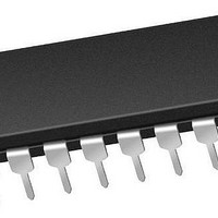
PIC24FV16KA301-E/P Microchip Technology, PIC24FV16KA301-E/P Datasheet - Page 71

PIC24FV16KA301-E/P
Manufacturer Part Number
PIC24FV16KA301-E/P
Description
16KB Flash, 2KB RAM, 512B EEPROM, 16 MIPS, 12-bit ADC, CTMU, 5V 20 PDIP .300in T
Manufacturer
Microchip Technology
Series
PIC® XLP™ 24Fr
Datasheet
1.PIC24F16KA301T-ISO.pdf
(320 pages)
Specifications of PIC24FV16KA301-E/P
Processor Series
PIC24FV
Core
PIC
Data Bus Width
16 bit
Program Memory Type
Flash
Program Memory Size
16 KB
Data Ram Size
2 KB
Maximum Operating Temperature
+ 125 C
Mounting Style
Through Hole
Package / Case
PDIP-20
Development Tools By Supplier
MPLAB IDE Software
Minimum Operating Temperature
- 40 C
Core Processor
PIC
Core Size
16-Bit
Speed
32MHz
Connectivity
I²C, IrDA, LIN, SPI, UART/USART
Peripherals
Brown-out Detect/Reset, HLVD, POR, PWM, WDT
Number Of I /o
17
Eeprom Size
512 x 8
Ram Size
2K x 8
Voltage - Supply (vcc/vdd)
3 V ~ 3.6 V
Data Converters
A/D 12x12b
Oscillator Type
Internal
Operating Temperature
-40°C ~ 125°C
Lead Free Status / Rohs Status
Details
- Current page: 71 of 320
- Download datasheet (3Mb)
6.4.1.1
To erase the entire data EEPROM (bulk erase), the
address registers do not need to be configured
because this operation affects the entire data
EEPROM. The following sequence helps in performing
a bulk erase:
1.
2.
3.
4.
5.
A typical bulk erase sequence is provided in
Example
EXAMPLE 6-3:
EXAMPLE 6-4:
2011 Microchip Technology Inc.
int __attribute__ ((space(eedata))) eeData = 0x1234;
Configure NVMCON to Bulk Erase mode.
Clear NVMIF status bit and enable NVM
interrupt (optional).
Write the key sequence to NVMKEY.
Set the WR bit to begin erase cycle.
Either poll the WR bit or wait for the NVM
interrupt (NVMIF set).
int newData;
unsigned int offset;
// Set up NVMCON to erase one word of data EEPROM
NVMCON = 0x4004;
// Set up a pointer to the EEPROM location to be erased
TBLPAG = __builtin_tblpage(&eeData);
offset = __builtin_tbloffset(&eeData);
__builtin_tblwtl(offset, newData);
asm volatile ("disi #5");
__builtin_write_NVM();
while(NVMCONbits.WR=1);
// Set up NVMCON to bulk erase the data EEPROM
NVMCON = 0x4050;
// Disable Interrupts For 5 Instructions
asm volatile ("disi #5");
// Issue Unlock Sequence and Start Erase Cycle
__builtin_write_NVM();
6-3.
Data EEPROM Bulk Erase
DATA EEPROM BULK ERASE
SINGLE-WORD WRITE TO DATA EEPROM
PIC24FV32KA304 FAMILY
6.4.2
To write a single word in the data EEPROM, the
following sequence must be followed:
1.
2.
3.
A typical single-word write sequence is provided in
Example
// Global variable located in EEPROM
// Initialize EE Data page pointer
// Initizlize lower word of address
// Write EEPROM data to write latch
// Disable Interrupts For 5 Instructions
// Issue Unlock Sequence & Start Write Cycle
// Optional: Poll WR bit to wait for
// New data to write to EEPROM
// write sequence to complete
Erase one data EEPROM word (as mentioned in
the
(NVMCON<12>) is set to ‘1’.
Write the data word into the data EEPROM
latch.
Program the data word into the EEPROM:
- Configure the NVMCON register to program one
- Clear NVMIF status bit and enable NVM
- Write the key sequence to NVMKEY.
- Set the WR bit to begin erase cycle.
- Either poll the WR bit or wait for the NVM
- To get cleared, wait until NVMIF is set.
EEPROM word (NVMCON<5:0> = 0001xx).
interrupt (optional).
interrupt (NVMIF set).
6-4.
previous
SINGLE-WORD WRITE
section)
if
PGMONLY
DS39995B-page 71
bit
Related parts for PIC24FV16KA301-E/P
Image
Part Number
Description
Manufacturer
Datasheet
Request
R

Part Number:
Description:
Manufacturer:
Microchip Technology Inc.
Datasheet:

Part Number:
Description:
Manufacturer:
Microchip Technology Inc.
Datasheet:

Part Number:
Description:
Manufacturer:
Microchip Technology Inc.
Datasheet:

Part Number:
Description:
Manufacturer:
Microchip Technology Inc.
Datasheet:

Part Number:
Description:
Manufacturer:
Microchip Technology Inc.
Datasheet:

Part Number:
Description:
Manufacturer:
Microchip Technology Inc.
Datasheet:

Part Number:
Description:
Manufacturer:
Microchip Technology Inc.
Datasheet:

Part Number:
Description:
Manufacturer:
Microchip Technology Inc.
Datasheet:


