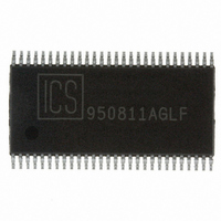
ICS950811AGLFT IDT, Integrated Device Technology Inc, ICS950811AGLFT Datasheet

ICS950811AGLFT
Specifications of ICS950811AGLFT
950811AGLFT
Available stocks
Related parts for ICS950811AGLFT
ICS950811AGLFT Summary of contents
Page 1
Integrated Circuit Systems, Inc. Frequency Generator with 200MHz Differential CPU Clocks Recommended Application: CK-408 clock for Brookdale-Mobile chipsets. Programmable for group to group skew. Output Features: • 3 Differential CPU Clock Pairs (differential current mode) • 7 PCI (3.3V) @ ...
Page 2
ICS950811 Pin Configuration ...
Page 3
Truth Table ...
Page 4
ICS950811 General I The information in this section assumes familiarity with I How to Write: • Controller (host) sends a start bit. • Controller (host) sends the write address D2 • ICS clock will acknowledge • Controller (host) sends a ...
Page 5
Byte 0: Control Register ...
Page 6
ICS950811 Byte 2: Control Register ...
Page 7
Byte 5: Programming Edge Rate (1 = enable disable ...
Page 8
ICS950811 Absolute Maximum Ratings Supply Voltage . . . . . . . . . . . . . . . . . . . . . . . . . 5.5 V Logic Inputs . . . . . ...
Page 9
Electrical Characteristics - CPU 70°C; VDD=3.3V +/-5 PARAMETER SYMBOL Current Source 1 Output Impedance Zo Output High Voltage V OH3 Output Low Voltage V OL3 Rise Time t r3 Fall Time t f3 Duty ...
Page 10
ICS950811 Electrical Characteristics - 3V66 70°C; VDD=3.3V +/-5 PARAMETER SYMBOL Output Frequency Output Impedance R V DSP1 O 1 Output High Voltage Output Low Voltage V ...
Page 11
Electrical Characteristics - REF 70°C; VDD=3.3V +/-5 PARAMETER SYMBOL Output Frequency Output Impedance R DSP1 1 Output High Voltage Output Low Voltage Output High Current ...
Page 12
ICS950811 Un-Buffered Mode 3V66 & PCI Phase Relationship All 3V66 clocks are pphase with each other. In the case where 3V66_1 is configured as 48MHz VCH clock, there is no defined phase relationship between 3V66_1/VCH and other ...
Page 13
Normal operation transition to Suspend State S1 Entry sequence of events: 1. Power-Down (PD#) pin is taken from a high to low to start into S1 Suspend state with digital filtering of the transition in the clock circuit. 2. The ...
Page 14
ICS950811 PCI_STOP# - Assertion (transition from logic "1" to logic "0") The impact of asserting the PCI_STOP# signal will be the following. All PCI[6:0] and stoppable PCI_F[2,0] clocks will latch low in their next high to low transition. The PCI_STOP# ...
Page 15
PD# - Assertion (transition from logic "1" to logic "0") When PD# is sampled low by two consecutive rising edges of CPU clock then all clock outputs except CPU clocks must be held low on their next high to low ...
Page 16
ICS950811 INDEX INDEX AREA AREA aaa 6.10 mm. Body, 0.50 mm. pitch TSSOP (0.020 mil) (240 mil) Ordering Information 950811yGLFT Example: XXXX ...
Page 17
Ordering Information 950811yFLFT Example: XXXX 0482E—08/09/07 SYMBOL α VARIATIONS N 56 Reference Doc.: JEDEC Publication 95, MO-118 10-0034 Designation for tape and reel ...
Page 18
ICS950811 Revision History Rev. Issue Date Description 1. Removed SSOP Package Information. D 12/21/06 2. Added LF Ordering Information. E 08/09/07 Added SSOP Package Information. 0482E—08/09/07 18 Page # 16 17 ...


