ICS950811AGLFT IDT, Integrated Device Technology Inc, ICS950811AGLFT Datasheet - Page 13
ICS950811AGLFT
Manufacturer Part Number
ICS950811AGLFT
Description
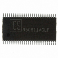
IC FREQ GEN 200MHZ CLK 56-TSSOP
Manufacturer
IDT, Integrated Device Technology Inc
Type
Frequency Generatorr
Datasheet
1.ICS950811AGLFT.pdf
(18 pages)
Specifications of ICS950811AGLFT
Frequency - Max
200MHz
Voltage - Supply
3.135 V ~ 3.465 V
Operating Temperature
0°C ~ 70°C
Mounting Type
Surface Mount
Package / Case
56-TSSOP
Frequency-max
200MHz
Lead Free Status / RoHS Status
Lead free / RoHS Compliant
Output
-
Input
-
Other names
800-1818-2
950811AGLFT
950811AGLFT
Available stocks
Company
Part Number
Manufacturer
Quantity
Price
Company:

Part Number:
ICS950811AGLFT
Manufacturer:
ICS
Quantity:
225
Part Number:
ICS950811AGLFT
Manufacturer:
ICS
Quantity:
20 000


Normal operation transition to Suspend State S1 Entry sequence of events:
Suspend State S1 Exit transition to normal operation sequence of events:
0482E—08/09/07
1. Power-Down (PD#) pin is taken from a high to low to start into S1 Suspend state with digital filtering of the
2. The first clocks to be forced to a Stop Low power down condition are the PCI buffer output clocks after a full
3. Immediately after the PCI clocks have been stopped the 66Buf_0:2 clocks are stopped low after the next
4. Following the two buffer output clocks being stopped (PCI then 66.6Buffer outputs), the remaining clocks
5. After the CPU PLL clocks are stopped, the 48 MHz clocks (USB, DOT clocks) will stop low, then the REF
6. After the clocks have all been stopped, the internal PLL stages and the Crystal oscillator will all be driven to
7. As a note to power management calculations, please be aware that the CPU design requires that in the
1. Power-Down (PD#) pin is taken from Low to High with digital filtering of the transition in the clock circuit to
2. The Crystal Oscillator and the two PLL stages are released from PD to start-up to normal operation. No
3. The CPU PLL clocks (differential CPU outputs and the driven 3V66_(0:1) clocks are operating first as soon
4. A delay is built into the clock generator that allows the CPU, driven 3V66_0,1 and the single buffer clock
5. The initial clocks released after the delay are the 66Buf_0, 2 outputs.
6. After the 66Buf_0,2 clocks are released, then the PCI clocks are released.
7. It will always be the sequence of 66_1 (pin 22) released with the CPU clocks, then after the delay the
8. Following the 66Buf_0,2 clocks, the 48 MHz (DOT and USB clocks) and the REF (14.318MHz) clocks are
9. Note, the initial power-up time is the same as this PD release, the PLL will power-up and the outputs will be
transition in the clock circuit.
clock cycle. If the PCI_Stop# is low, then the free-running PCI clocks (for PCI and APIC signals) are the
remaining PCI buffer clocks stopped.
high to low transition. It will always be a sequence of PCI stopping, THEN the 66Buf clocks.
within a short delay will transition to a stopped power-down state. The first of these driven clocks that
transition to a stopped state are all of the CPU PLL clocks: the CPU and the driven 3V66 clocks.
clock 14.318 MHz clock will stop low.
a low power stopped condition.
Power-Down (S1 mode) the CPU outputs have a differential bias voltage driving the differential input stage of
the CPU in this S1 state. For this PD condition of the clock generator, the IDD_PD is running around 30 to
45 mA from having the Iref running (5 mA), the output multiplier bias generator at a 2X condition and the
output current source outputs are running at a 2xIref bias level (for approx 10 mA each CPU output). This
results in a higher level of Clock generator IDD_PD than in prior generations of clocks due to the CPU output
differential requirements.
return to normal running operation.
clocks will operate until the Lock detect circuitry verifies the PLL has reached stable final frequency (the
same as normal initial power-up).
as the Lock detect releases the clocks.
output (at pin 22) is also released from the PD stopped state (but NOT the other 66Buf0,2 and not the PCI
outputs). This allows the GMCH chipset 66.6 MHz DLL stage to start operating and have an operating
feedback path before the other buffer outputs are released. This change is why the requirement is made that
pin 22 be the connection from the clock to the GMCH chipset.
PCI clocks, the 48 MHz and REF (14.318 MHz) clocks are also NOT released at this point.
66Buf_1 (at pin 22) to operate before other clocks are released. This delay is larger than 30 uS and shorter
than 400 uS, and after this the other clocks are staged for a sequential release.
remaining 66Buf_0,2 first, THEN the PCI clocks.
released.
running within a 3 ms time point.
With the release of these clocks, the single 66Buf_1 buffer driven
13
Note that along with the 66Buf_0,2 and the
ICS950811
Related parts for ICS950811AGLFT
Image
Part Number
Description
Manufacturer
Datasheet
Request
R

Part Number:
Description:
TRANSLATION DEVICE DPI 80-PQFP
Manufacturer:
IDT, Integrated Device Technology Inc
Datasheet:
Part Number:
Description:
IDT PART
Manufacturer:
IDT, Integrated Device Technology Inc
Datasheet:
Part Number:
Description:
IC LIU T1/E1/J1 OCTAL 256PBGA
Manufacturer:
IDT, Integrated Device Technology Inc
Datasheet:

Part Number:
Description:
IC FREQ TIMING GENERATOR 28TSSOP
Manufacturer:
IDT, Integrated Device Technology Inc
Datasheet:
Part Number:
Description:
IC CLK DVR PLL 1:10 40VFQFPN
Manufacturer:
IDT, Integrated Device Technology Inc
Datasheet:
Part Number:
Description:
IC CLK FANOUT BUFFER 1:18 32LQFP
Manufacturer:
IDT, Integrated Device Technology Inc
Datasheet:
Part Number:
Description:
IC CLK FANOUT BUFFER 1:18 32LQFP
Manufacturer:
IDT, Integrated Device Technology Inc
Datasheet:
Part Number:
Description:
IC CK505 VREG/RES 56TSSOP
Manufacturer:
IDT, Integrated Device Technology Inc
Datasheet:

Part Number:
Description:
IC SDRAM CLK DVR 1:10 48-TSSOP
Manufacturer:
IDT, Integrated Device Technology Inc
Datasheet:

Part Number:
Description:
IC CLK DVR PLL 1:10 48TSSOP
Manufacturer:
IDT, Integrated Device Technology Inc
Datasheet:
Part Number:
Description:
IC FLEXPC CLK PROGR P4 56-TSSOP
Manufacturer:
IDT, Integrated Device Technology Inc
Datasheet:
Part Number:
Description:
IC FLEXPC CLK PROGR P4 56-TSSOP
Manufacturer:
IDT, Integrated Device Technology Inc
Datasheet:
Part Number:
Description:
IC FLEXPC CLK PROGR P4 56-SSOP
Manufacturer:
IDT, Integrated Device Technology Inc
Datasheet:

Part Number:
Description:
IC PLL CLK DRIVER 2.5V 28-TSSOP
Manufacturer:
IDT, Integrated Device Technology Inc
Datasheet:
Part Number:
Description:
IC CLOCK DRIVER 2.5V 24-TSSOP
Manufacturer:
IDT, Integrated Device Technology Inc
Datasheet: