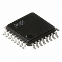
PCK9446BD,128 NXP Semiconductors, PCK9446BD,128 Datasheet - Page 8

PCK9446BD,128
Manufacturer Part Number
PCK9446BD,128
Description
IC CLOCK BUFFER FANOUT 32LQFP
Manufacturer
NXP Semiconductors
Type
Fanout Buffer (Distribution), Divider, Multiplexerr
Datasheet
1.PCK9446BD151.pdf
(17 pages)
Specifications of PCK9446BD,128
Number Of Circuits
1
Ratio - Input:output
2:10
Differential - Input:output
No/No
Input
LVCMOS
Output
LVCMOS
Frequency - Max
250MHz
Voltage - Supply
2.375 V ~ 3.465 V
Operating Temperature
-40°C ~ 85°C
Mounting Type
Surface Mount
Package / Case
32-LQFP
Frequency-max
250MHz
Lead Free Status / RoHS Status
Lead free / RoHS Compliant
Other names
935280839128
PCK9446BD-F
PCK9446BD-F
PCK9446BD-F
PCK9446BD-F
Available stocks
Company
Part Number
Manufacturer
Quantity
Price
Company:
Part Number:
PCK9446BD,128
Manufacturer:
NXP Semiconductors
Quantity:
10 000
Philips Semiconductors
Table 10.
T
[1]
Table 11.
T
[1]
[2]
PCK9446_1
Product data sheet
Symbol
f
f
t
t
t
t
t
t
t
t
t
t
t
Symbol
t
t
t
ref
o(max)
PLH
PHL
PLZ
PHZ
PZL
PZH
sk(o)
sk(pr)
sk(p)
r
f
sk(o)
sk(pr)
sk(p)
amb
amb
ref
o
o
Dynamic (AC) characteristics apply for parallel output termination of 50
Dynamic (AC) characteristics apply for parallel output termination of 50
For all other dynamic (AC) specifications, refer to 2.5 V or 3.3 V tables according to the supply voltage of the output bank.
= 40 C to +85 C; V
= 40 C to +85 C; V
Dynamic characteristics (2.5 V)
Dynamic characteristics (mixed supply voltages)
Parameter
reference frequency
maximum output frequency
reference duty cycle
LOW-to-HIGH propagation delay
HIGH-to-LOW propagation delay
LOW to OFF-state propagation delay
HIGH to OFF-state propagation delay
OFF-state to LOW propagation delay
OFF-state to HIGH propagation delay
output skew time
process skew time
pulse skew time
output duty cycle
rise time
fall time
Parameter
output skew time
process skew time
pulse skew time
output duty cycle
CC
CC
= V
= 3.3
CC(bankA)
Conditions
output-to-output
part-to-part
output
1 or
5 %; any V
within one bank
any output bank; same output divider
any output; any output divider
= V
2 output;
CC(bankB)
CC(bankA)
Rev. 01 — 10 April 2006
Conditions
input
input
CLKn to any Q
CLKn to any Q
output-to-output
part-to-part
output
input; CLK0, CLK1;
0.7 V to 1.7 V
output; 0.6 V to 1.8 V
input; CLK0, CLK1;
1.7 V to 0.7 V
output; 1.8 V to 0.6 V
1 output; FSELx = 0
2 output; FSELx = 1
1 or
within one bank
any output bank,
same output divider
any output,
any output divider
ref
= V
, V
= 50 %
CC(bankC)
CC(bankB)
2 output;
= 2.5 V
, V
to V
to V
ref
CC(bankC)
2.5 V and 3.3 V LVCMOS clock fan-out buffer
= 50 %
T
T
.
.
5 %.
= 2.5 V
[1]
Min
-
-
-
-
-
45
Min
0
0
0
25
2.2
2.2
-
-
-
-
-
45
-
0.1
-
0.1
5 % or 3.3 V
© Koninklijke Philips Electronics N.V. 2006. All rights reserved.
Typ
-
-
-
-
-
50
Typ
250
250
125
-
-
-
-
-
-
-
-
50
-
-
-
-
PCK9446
5 %.
Max
150
200
1.2
3.0
500
55
Max
-
-
-
75
5.0
5.0
10
10
10
10
150
200
1.2
3.0
500
55
3.0
1.0
3.0
1.0
[1][2]
Unit
ps
ps
ns
ns
ps
%
Unit
MHz
MHz
MHz
%
ns
ns
ns
ns
ns
ns
ps
ps
ns
ns
ps
%
ns
ns
ns
ns
8 of 17


