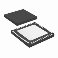
LMK04001BISQE/NOPB National Semiconductor, LMK04001BISQE/NOPB Datasheet - Page 33

LMK04001BISQE/NOPB
Manufacturer Part Number
LMK04001BISQE/NOPB
Description
IC CLOCK COND 1.5GHZ W/PLL 48LLP
Manufacturer
National Semiconductor
Series
PowerWise®r
Type
Clock Conditionerr
Datasheet
1.LMK04010BISQENOPB.pdf
(54 pages)
Specifications of LMK04001BISQE/NOPB
Pll
Yes
Input
LVCMOS
Output
LVCMOS, 2VPECL, LVPECL
Number Of Circuits
1
Ratio - Input:output
2:7
Differential - Input:output
Yes/Yes
Frequency - Max
1.57GHz
Divider/multiplier
Yes/Yes
Voltage - Supply
3.15 V ~ 3.45 V
Operating Temperature
-40°C ~ 85°C
Mounting Type
Surface Mount
Package / Case
48-LLP
Frequency-max
1.57GHz
Lead Free Status / RoHS Status
Lead free / RoHS Compliant
Other names
LMK04001BISQETR
Available stocks
Company
Part Number
Manufacturer
Quantity
Price
Company:
Part Number:
LMK04001BISQE/NOPB
Manufacturer:
NS
Quantity:
250
16.3 REGISTER R0 TO R4
Registers R0 through R4 control the five clock outputs. Reg-
ister R0 controls CLKout0, Register R1 controls CLKout1, and
so on. Aside from this, the functions of the bits in these reg-
isters are identical. The X in CLKoutX_MUX, CLKoutX_DIV,
CLKoutX_DLY, and CLKoutX_EN denote the actual clock
output which may be from 0 to 4.
16.3.1 CLKoutX_DIV: Clock Channel Divide Registers
Each of the five clock output channels (0 though 4) has a
dedicated 8-bit divider followed by a fixed divide by 2 that is
used to generate even integer related versions of the distri-
bution path clock frequency (VCO Divider output). If the VCO
Divider value is even then the Channel Divider may be by-
passed (See CLK Output Mux), giving an effective divisor of
1 while preserving a 50% duty cycle output waveform.
16.3.2 EN_CLKoutX: Clock Channel Output Enable
Each Clock Output Channel may be either enabled or dis-
abled via the Clock Output Enable control bits. Each output
enable control bit is gated with the Global Output Enable input
pin (GOE) and Global Output Enable bit (EN_CLKout_Glob-
al). The GOE pin provides an internal pull-up so that if it is
unterminated externally, the clock output states are deter-
mined by the Clock Output Enable Register bits. All clock
outputs can be set to the low state simultaneously if the GOE
pin is pulled low by an external signal. If EN_CLKout_Global
is programmed to 0 all outputs are turned off. If both GOE and
EN_CLKout_Global are low the clock outputs are turned off.
Note the default state of CLKout2 is ON after power on or
RESET assertion. The nominal frequency is 62 MHz
(LMK040x1) or 81 MHz (LMK040x3). This is based on a
channel divide value of 12 and default VCO_DIV value of 2.
If an active CLKout2 at power on is inappropriate for the user’s
application, the following method can be employed to shut off
CLKout2 during system initialization:
b7 b6 b5 b4 b3 b2 b1
EN_CLKout0
EN_CLKout1
EN_CLKout2
EN_CLKout3
EN_CLKout4
EN_CLKout_
TABLE 3. CLKoutX_DIV: Clock Channel Divide Values
TABLE 4. EN_CLKoutX: Clock Channel Output Enable
0
0
0
0
0
0
1
-
BIT NAME
Global
0
0
0
0
0
0
1
-
CLKoutX_DIV [ 7:0 ]
0
0
0
0
0
0
1
-
0
0
0
0
0
0
1
-
According to
individual
--
0
0
0
0
0
0
1
channel
settings
BIT = 1
ON
ON
ON
ON
ON
0
0
0
0
1
1
1
-
Control Bits
0
0
1
1
0
0
1
-
EN_CLKout
b0
0
1
0
1
0
1
1
X = OFF
-
BIT = 0
OFF
OFF
OFF
OFF
OFF
All
Total Divide Value
invalid
510
10
DEFAULT
2
4
6
8
-
OFF
OFF
OFF
OFF
ON
-
33
•
16.3.3 CLKoutX_DLY: Clock Channel Phase Delay
Adjustment
Each output channel has an output delay register that can be
used to introduce a lag relative to the distribution path fre-
quency (VCO Divider output). These registers support a 150
ps stepsize and range from 0 to 2.25 ns of total delay. When
the channel phase delay registers are enabled, a nominal
fixed delay of 300 ps of delay is incurred in addition to the
programmed delay. The Channel Phase Delay Adjustment
Registers are 4 bits wide and are programmed as follows:
16.3.4 CLKoutX/CLKoutX* LVCMOS Mode Control
For clock outputs that are configured as LVCMOS, the LVC-
MOS CLKoutX/CLKoutX* outputs can be independently con-
figured by uWire CLKoutXA_STATE and CLKoutXB_STATE
bits. The following choices are available for LVCMOS outputs:
TABLE 6. CLKoutXA_STATE, CLKoutXB_STATE Control
TABLE 5. CLKoutX_DLY: Clock Channel Delay Control
CLKoutXA_STATE
When the device is powered on, holding the GOE pin LOW
will disable all clock outputs. The device can be
programmed while the GOE is held LOW. The state of
CLKout2 can be altered during device programming
according to the user’s specific application needs. After
device configuration is complete, the GOE pin should be
set HIGH to enable the active clock channels.
b3
b1
0
0
0
0
0
0
0
0
1
1
1
1
1
1
1
1
0
0
1
1
CLKoutX_DLY [ 3:0 ]
b2
b0
Bits for LVCMOS Modes
0
0
0
0
1
1
1
1
0
0
0
0
1
1
1
1
0
1
0
1
Bit Values
CLKoutXB_STATE
b1
b1
0
0
1
1
0
0
1
1
0
0
1
1
0
0
1
1
0
0
1
1
b0
b0
0
1
0
1
0
1
0
1
0
1
0
1
0
1
0
1
0
1
0
1
www.national.com
LVCMOS
Inverted
DELAY
Modes
Normal
STATE
1050
1200
1350
1500
1650
1800
1950
2100
2250
TRI-
(ps)
Low
150
300
450
600
750
900
0


