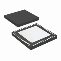
LMK04001BISQE/NOPB National Semiconductor, LMK04001BISQE/NOPB Datasheet - Page 37

LMK04001BISQE/NOPB
Manufacturer Part Number
LMK04001BISQE/NOPB
Description
IC CLOCK COND 1.5GHZ W/PLL 48LLP
Manufacturer
National Semiconductor
Series
PowerWise®r
Type
Clock Conditionerr
Datasheet
1.LMK04010BISQENOPB.pdf
(54 pages)
Specifications of LMK04001BISQE/NOPB
Pll
Yes
Input
LVCMOS
Output
LVCMOS, 2VPECL, LVPECL
Number Of Circuits
1
Ratio - Input:output
2:7
Differential - Input:output
Yes/Yes
Frequency - Max
1.57GHz
Divider/multiplier
Yes/Yes
Voltage - Supply
3.15 V ~ 3.45 V
Operating Temperature
-40°C ~ 85°C
Mounting Type
Surface Mount
Package / Case
48-LLP
Frequency-max
1.57GHz
Lead Free Status / RoHS Status
Lead free / RoHS Compliant
Other names
LMK04001BISQETR
Available stocks
Company
Part Number
Manufacturer
Quantity
Price
Company:
Part Number:
LMK04001BISQE/NOPB
Manufacturer:
NS
Quantity:
250
Internal loop filter capacitors for C3 and C4 can be set indi-
vidually according to the following table.
16.10.7 PLL1 CP TRI-STATE and PLL2 CP TRI-STATE
The charge pump output of either CPout1 or CPout2 may be
placed in a TRI-STATE mode by setting the appropriate PLLx
CP TRI-STATE bit.
PLL2_C3_C4_
b3 b2 b1 b0
TABLE 22. PLL2 Internal Loop Filter Capacitor Values
0
0
0
0
0
0
0
0
1
1
1
1
1
1
1
1
TABLE 20. PLL2 Internal Loop Filter Resistor Values,
TABLE 21. PLL2 Internal Loop Filter Resistor Values,
LF [3:0]
0
0
0
0
1
1
1
1
0
0
0
0
1
1
1
1
b2
b2
0
0
0
0
1
1
1
1
0
0
0
0
1
1
1
1
0
0
1
1
0
0
1
1
0
0
1
1
0
0
1
1
PLL2_R3_LF [2:0]
PLL2_R4_LF [2:0]
0
1
0
1
0
1
0
1
0
1
0
1
0
1
0
1
b1
b1
0
0
1
1
0
0
1
1
0
0
1
1
0
0
1
1
Loop Filter Capacitance (pF)
PLL2_R3_LF
PLL2_R4_LF
C3 = 100, C4 = 110
C3 = 150, C4 = 110
C3 = 50, C4 = 110
C3 = 50, C4 = 160
C3 = 100, C4 = 10
C3 = 100, C4 = 60
C3 = 150, C4 = 60
C3 = 50, C4 = 10
C3 = 0, C4 = 110
C3 = 0, C4 = 160
C3 = 0, C4 = 10
C3 = 0, C4 = 60
Reserved
Reserved
Reserved
Reserved
b0
b0
0
1
0
1
0
1
0
1
0
1
0
1
0
1
0
1
RESISTANCE
RESISTANCE
< 600 Ω
< 200 Ω
Invalid
Invalid
Invalid
Invalid
Invalid
Invalid
10 kΩ
20 kΩ
30 kΩ
40 kΩ
10 kΩ
20 kΩ
30 kΩ
40 kΩ
37
16.11 REGISTER 14
16.11.1 OSCin_FREQ: PLL2 Oscillator Input Frequency
Register
The frequency of the PLL2 reference input to the PLL2 Phase
Detector (OSCin/OSCin* port) must be programmed in order
to support proper operation of the internal VCO tuning algo-
rithm. This is an 8-bit register that sets the frequency to the
nearest 1-MHz increment.
16.11.2 PLL2_R: PLL2_R Counter
The PLL2 R Counter is 12 bits wide. It divides the PLL2 OS-
Cin/OSCin* clock and is connected to the PLL2 Phase De-
tector.
16.11.3 PLL_MUX: LD Pin Selectable Output
The signal appearing on the LD pin is programmable via the
uWire interface and provides access to several internal sig-
nals which may be valuable for either status monitoring during
normal operation or for debugging during the hardware de-
velopment phase. This pin may be forced to either a HIGH or
LOW state, and may also be configured as specified in Table
27.
b11 b10 b9 b8 b7 b6 b5 b4 b3 b2 b1 b0
b7
TABLE 23. PLL1 Charge Pump TRI-STATE bit values
TABLE 24. PLL2 Charge Pump TRI-STATE bit values
0
0
1
0
0
0
1
1
1
.
PLL1 CP TRI-STATE
PLL2 CP TRI-STATE
TABLE 26. PLL2_R: PLL2_R Counter Values
b6
0
0
1
0
0
0
1
1
1
TABLE 25. OSCin_FREQ Register Values
.
.
0
0
1
.
OSCin_FREQ [7:0]
b5
0
0
0
1
0
1
.
.
1
0
1
0
0
0
1
.
b4
0
0
0
1
0
1
.
.
0
0
1
.
R [11:0]
0
0
1
.
b3
0
0
0
1
1
1
.
.
0
0
1
.
b2
0
0
0
0
0
1
.
.
0
0
1
.
PLL1 CPout1 is at TRI-
PLL2 CPout2 is at TRI-
PLL1 CPout1 is active
PLL2 CPout2 is active
b1
0
0
1
.
0
0
1
1
0
1
.
.
Description
Description
0
0
1
.
STATE
STATE
b0
0
1
0
0
1
1
.
.
0
0
1
.
www.national.com
Not Valid
Not Valid
Not Valid
250 MHz
0
1
1
.
VALUE
1 MHz
2 MHz
VALUE
...
.
Valid
4095
Not
...
1


