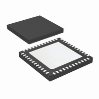
LMK04001BISQE/NOPB National Semiconductor, LMK04001BISQE/NOPB Datasheet - Page 40

LMK04001BISQE/NOPB
Manufacturer Part Number
LMK04001BISQE/NOPB
Description
IC CLOCK COND 1.5GHZ W/PLL 48LLP
Manufacturer
National Semiconductor
Series
PowerWise®r
Type
Clock Conditionerr
Datasheet
1.LMK04010BISQENOPB.pdf
(54 pages)
Specifications of LMK04001BISQE/NOPB
Pll
Yes
Input
LVCMOS
Output
LVCMOS, 2VPECL, LVPECL
Number Of Circuits
1
Ratio - Input:output
2:7
Differential - Input:output
Yes/Yes
Frequency - Max
1.57GHz
Divider/multiplier
Yes/Yes
Voltage - Supply
3.15 V ~ 3.45 V
Operating Temperature
-40°C ~ 85°C
Mounting Type
Surface Mount
Package / Case
48-LLP
Frequency-max
1.57GHz
Lead Free Status / RoHS Status
Lead free / RoHS Compliant
Other names
LMK04001BISQETR
Available stocks
Company
Part Number
Manufacturer
Quantity
Price
Company:
Part Number:
LMK04001BISQE/NOPB
Manufacturer:
NS
Quantity:
250
www.national.com
17.1 System Level Diagram (continued)
Figure 3 shows an LMK04000 family device with external cir-
cuitry. The primary reference clock input is at CLKin0/0*. A
secondary reference clock is driving CLKin1/1*. Both clocks
are depicted as AC coupled differential drivers. The VCXO
attached to the OSCin/OSCin* port is configured as an AC
coupled single-ended driver. Any of the input ports
(CLKin0/0*, CLKin1/1*, or OSCin/OSCin*) may be configured
as either differential or single-ended. These options are dis-
cussed later in the data sheet.
The diagram shows an optional connection between the LD
pin and GOE. With this arrangement, the LD pin can be pro-
grammed to output a lock detect signal that is active HIGH
(see Table 27 for optional LD pin outputs). If lock is lost, the
LD pin will transition to a LOW, pulling GOE low and causing
all clock outputs to be disabled. This scheme should be used
only if disabling the clock outputs is desirable when lock is
lost.
The loop filter for PLL2 consists of three external components
that implement two lower order poles, plus optional internal
integrated components if 3rd or 4th order poles are needed.
The loop filter components for PLL1 must be external com-
ponents.
The VCO output buffer signal that appears at the Fout pin
when enabled (EN_Fout = 1) should be AC coupled using a
100 pF capacitor. This output is a single-ended signal by de-
fault. If a differential signal is required, a 50 Ω balun may be
connected to this pin to convert it to differential.
The clock outputs are all AC coupled with 0.1 µF capacitors.
CLKout1 and CLKout3 are depicted as LVPECL, with 120 Ω
emitter resistors as source termination. However, the output
format of the clock channels will vary by device part number,
so the designer should use the appropriate source termina-
tion for each channel. Later sections of this data sheet illus-
trate alternative methods for AC coupling, DC coupling and
terminating the clock outputs.
17.2 LDO BYPASS AND BIAS PIN
The LDObyp1 and LDObyp2 pins should be connected to
GND through external capacitors, as shown in the diagram.
Furthermore, the Bias pin should be connected to V
through a 1 µF capacitor in series.
17.3 LOOP FILTER
Each PLL of the LMK04000 family requires a dedicated loop
filter. The loop filter for PLL1 must be connected to the CPout1
CC
40
pin. Figure 4 shows a simple 2-pole loop filter. The output of
the filter drives an external VCXO module or discrete imple-
mentation of a VCXO using a crystal resonator. Higher order
loop filters may be implemented using additional external R
and C components. It is recommended the loop filter for PLL1
result in a total closed loop bandwidth in the range of 10 Hz
to 200 Hz. The design of the loop filter is application specific
and highly dependent on parameters such as the phase noise
of the reference clock, VCXO phase noise, and phase detec-
tor frequency for PLL1. National’s Clock Conditioner Owner’s
Manual covers this topic in detail and National’s Clock Design
Tool can be used to simulate loop filter designs for both PLLs.
These resources may be found: http://www.national.com/tim-
ing/.
As shown in the diagram, the charge pump for PLL2 is directly
connected to the optional internal loop filter components,
which are normally used only if either a third or fourth pole is
needed. The first and second poles are implemented with ex-
ternal components. The loop must be designed to be stable
over the entire application-specific tuning range of the VCO.
The designer should note the range of K
of Electrical Characteristics and how this value can change
over the expected range of VCO tuning frequencies. Because
loop bandwidth is directly proportional to K
should model and simulate the loop at the expected extremes
of the desired tuning range, using the appropriate values for
K
When designing with the integrated loop filter of the
LMK04000 family, considerations for minimum resistor ther-
mal noise often lead one to the decision to design for the
minimum value for integrated resistors, R3 and R4. Both the
integrated loop filter resistors and capacitors (C3 and C4) also
restrict the maximum loop bandwidth. However, these inte-
grated components do have the advantage that they are
closer to the VCO and can therefore filter out some noise and
spurs better than external components. For this reason, a
common strategy is to minimize the internal loop filter resis-
tors and then design for the largest internal capacitor values
that permit a wide enough loop bandwidth. In situations where
spurs requirements are very stringent and there is margin on
phase noise, it might make sense to design for a loop filter
with integrated resistor values larger than their minimum val-
ue.
VCO
.
VCO
VCO
listed in the table
, the designer


