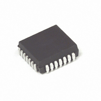
MC88915TFN70R2 Freescale Semiconductor, MC88915TFN70R2 Datasheet

MC88915TFN70R2
Specifications of MC88915TFN70R2
Available stocks
Related parts for MC88915TFN70R2
MC88915TFN70R2 Summary of contents
Page 1
SEMICONDUCTOR TECHNICAL DATA 55, 70, 100, 133 and 160MHz Versions The MC88915T Clock Driver utilizes phase–locked loop technology to lock its low skew outputs’ frequency and phase onto an input reference clock designed to provide clock distribution for ...
Page 2
PIN SUMMARY 2 Pinout: 28–Lead PLCC (Top View) FN SUFFIX PLASTIC PLCC CASE 776–02 MOTOROLA ...
Page 3
Figure 1. MC88915T Block Diagram (All Versions) MOTOROLA 3 ...
Page 4
MC88915TFN55 and MC88915TFN70 SYNC INPUT TIMING REQUIREMENTS Symbol t ,SYNC Inputs Rise/Fall Time, SYNC Inputs RISE/FALL From 0 SYNC Inputs Input Clock Period SYNC Inputs CYCLE Duty Cycle SYNC Inputs Input Duty Cycle SYNC Inputs 1. ...
Page 5
MC88915TFN55 and MC88915TFN70 FREQUENCY SPECIFICATIONS (T =– + Symbol 1 f Maximum Operating Frequency (2X_Q Output) max Maximum Operating Frequency (Q0–Q4,Q5 Output) 1. Maximum Operating Frequency is guaranteed with the part in a phase–locked condition, ...
Page 6
SYNC INPUT TIMING REQUIREMENTS Symbol t ,SYNC Inputs Rise/Fall Time, SYNC Inputs From 0.8 to 2.0V RISE/FALL t , SYNC Inputs Input Clock Period SYNC Inputs CYCLE Duty Cycle SYNC Inputs Input Duty Cycle SYNC Inputs 1. These t minimum ...
Page 7
AC CHARACTERISTICS (T =– + Symbol Parameter t Rise/Fall Time, All Outputs RISE/FALL Outputs (Between 0.2V and 0. Rise/Fall Time Into a 20pF Load, With Ter- RISE/FALL 2X_Q Output mination Specified in ...
Page 8
SYNC INPUT TIMING REQUIREMENTS Symbol t ,SYNC Inputs Rise/Fall Time, SYNC Inputs From 0.8 to 2.0V RISE/FALL t , SYNC Inputs Input Clock Period SYNC Inputs CYCLE Duty Cycle SYNC Inputs Input Duty Cycle SYNC Inputs 1. These t minimum ...
Page 9
AC CHARACTERISTICS (T =– + Symbol Parameter t Rise/Fall Time, All Outputs RISE/FALL Outputs (Between 0.2V and 0. Rise/Fall Time Into a 20pF Load, With Ter- RISE/FALL 2X_Q Output mination Specified in ...
Page 10
SYNC INPUT TIMING REQUIREMENTS Symbol t ,SYNC Inputs Rise/Fall Time, SYNC Inputs From 0.8 to 2.0V RISE/FALL t , SYNC Inputs Input Clock Period SYNC Inputs CYCLE Duty Cycle SYNC Inputs Input Duty Cycle SYNC Inputs 1. These t minimum ...
Page 11
AC CHARACTERISTICS ( + Symbol Parameter t Rise/Fall Time, All Outputs RISE/FALL Outputs (Between 0.2V and 0. Rise/Fall Time RISE/FALL 2X_Q Output t Output Pulse Width: Q0, Q1, Q2, Q3, Q4, PULSE ...
Page 12
Applications Information for All Versions General AC Specification Notes 1. Several specifications can only be measured when the MC88915TFN55, 70 and 100 are in phase–locked operation not possible to have the part in phase–lock on ATE (automated test ...
Page 13
Figure 2. Depiction of the Fixed SYNC to Feedback Offset (tPD) Which is Present When The t specification guarantees that the rising edges SKEWr of outputs Q/2, Q0, Q1, Q2, Q3, and Q4 will always fall within ...
Page 14
Calculation of Total Output–to–Skew between multiple parts (Part–to–Part skew) By combining the t specification and the information in PD Note 5, the worst case output–to–output skew between multiple 88915’s connected in parallel can be calculated. This calculation assumes that ...
Page 15
The lock indicator pin (LOCK) will reliably indicate a phase–locked condition at SYNC input frequencies down to 10MHz. At frequencies below 10MHz, the frequency of correction pulses going into the phase detector form the SYNC and FEEDBACK pins may ...
Page 16
Figure 4. Output/Input Switching Waveforms and Timing Diagrams (These waveforms represent the hook–up configuration of Figure 5a on page 17) Timing Notes: The MC88915T aligns rising edges of the FEEDBACK input and SYNC input, therefore the SYNC input does not ...
Page 17
Figure 5a. Wiring Diagram and Frequency Relationships With Q/2 Output Feed Back Figure 5b. Wiring Diagram and Frequency Relationships With Q4 Output Feed Back Figure 5c. Wiring Diagram and Frequency Relationships with 2X_Q Output Feed Back MOTOROLA 17 ...
Page 18
Figure 6. Recommended Loop Filter and Analog Isolation Scheme for the MC88915T Notes Concerning Loop Filter and Board Layout Issues 1. Figure 6 shows a loop filter and analog isolation scheme which will be effective in most applications. The following ...
Page 19
Figure 7. Representation of a Potential Multi–Processing Application Utilizing the MC88915T for Frequency Multiplication and Low Board–to–Board Skew MC88915T System Level Testing Functionality 3–state functionality has been added to the 100MHz version of the MC88915T to ease system board testing. ...
Page 20
OUTLINE DIMENSIONS FN SUFFIX PLASTIC PACKAGE CASE 776–02 ISSUE BRK –M– VIEW D– –T– VIEW S VIEW ...
Page 21
Motorola reserves the right to make changes without further notice to any products herein. Motorola makes no warranty, representation or guarantee regarding the suitability of its products for any particular purpose, nor does Motorola assume any liability arising out of ...


