LMX2324SLBX National Semiconductor, LMX2324SLBX Datasheet - Page 7
LMX2324SLBX
Manufacturer Part Number
LMX2324SLBX
Description
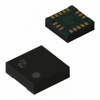
IC FREQ SYNTH 2.0GHZ 16LAMINATE
Manufacturer
National Semiconductor
Series
PLLatinum™r
Type
PLL Frequency Synthesizerr
Datasheet
1.LMX2324TM.pdf
(14 pages)
Specifications of LMX2324SLBX
Pll
Yes
Input
CMOS, TTL
Output
Clock
Number Of Circuits
1
Ratio - Input:output
1:1
Differential - Input:output
No/No
Frequency - Max
2GHz
Divider/multiplier
Yes/No
Voltage - Supply
2.7 V ~ 5.5 V
Operating Temperature
-40°C ~ 85°C
Mounting Type
Surface Mount
Package / Case
16-Laminate CSP
Frequency-max
2GHz
Lead Free Status / RoHS Status
Contains lead / RoHS non-compliant
Other names
LMX2324SLBX
LMX2324SLBXTR
LMX2324SLBXTR
Available stocks
Company
Part Number
Manufacturer
Quantity
Price
Company:

Part Number:
LMX2324SLBX
Manufacturer:
TI
Quantity:
1 456


Register
CP_TRI
PD_POL
TEST
R Divider Output
N Divider Output
Divide
2.2 R REGISTER
If the Address Bit (ADDR) is 1, when LE is transitioned high data is transferred from the 18-bit shift register into the 14-bit R register.
The R register contains a latch which sets the PLL 10-bit R counter divide ratio. The divide ratio is programmed using the bits
R_CNTR as shown in table 2.2.1. The ratio must be
charge pump TRI-STATE, and test mode respectively, as shown in 2.2.2. The RS bit is reserved and should always be set to zero.
X denotes a don't care condition. Data is clocked into the shift register MSB first.
2.2.1 10-Bit Programmable Reference Divider Ratio (R Counter)
Notes: Divide ratio: 2 to 1,023 (Divide ratios less than 2 are prohibited)
R_CNTR—These bits select the divide ratio of the programmable reference dividers.
2.2.2 R Register Truth Table
If the test mode is NOT activated (R[13]=0), the charge pump is active when CP_TRI is set LOW. When CP_TRI is set HIGH, the
charge pump output and phase comparator are forced to a TRI-STATE condition. This bit must be set HIGH if the test mode is
ACTIVATED (R[13]=1).
If the test mode is NOT activated (R[13]=0), PD_POL sets the VCO characteristics to positive when set HIGH. When PD_POL is
set LOW, the VCO exhibits a negative characteristic where the VCO frequency decreases with increasing control voltage.
If the test mode is ACTIVATED (R[13]=1), the outputs of the N and R counters are directed to the CP
The PD_POL bit selects which counter output according to Table 2.2.3.
2.2.3 Test Mode Truth Table (R[13] = 1)
Ratio
1,023
2
3
•
R
Bit
MSB
R16 R15 R14
17
CP
X
R9
0
0
1
•
o
Output
16
X
15
R[10]
R[11]
R[13]
X
R8
0
0
1
•
TEST
R13
14
Location
101030 Version 8 Revision 1
R12
RS
R7
13
0
0
1
•
PD_
POL
R11
12
R6
Charge Pump TRI-
STATE
Phase Detector Polarity
Test Mode Bit
0
0
1
≥
•
SHIFT REGISTER BIT LOCATION
2. The PD_POL, CP_TRI and TEST bits control the phase detector polarity,
CP_TRI R[10]
R_CNTR[9:0]
CP_
R10
TRI
11
Function
Print Date/Time: 2010/03/17 20:00:58
R5
Data Field
0
0
1
1
1
7
•
R9
10
R8
9
R4
0
0
1
•
R7
Normal Operation
Negative
Normal Operation
8
R6
7
R3
0
0
1
•
R5
R_CNTR[9:0]
6
0
R4
5
R2
R3
0
0
1
•
4
o
PD_POL R[11]
output to allow for testing.
TRI-STATE
Positive
Test Mode
R2
3
0
1
R1
R1
1
1
1
•
2
www.national.com
1
R0
1
R0
0
1
1
•
ADDR
LSB
Field
0
1
Related parts for LMX2324SLBX
Image
Part Number
Description
Manufacturer
Datasheet
Request
R

Part Number:
Description:
Pllatinum? 2.0 Ghz Frequency Synthesizer For Rf Personal Communications
Manufacturer:
National Semiconductor Corporation
Datasheet:

Part Number:
Description:
National Semiconductor [8-Bit D/A Converter]
Manufacturer:
National Semiconductor
Datasheet:
Part Number:
Description:
National Semiconductor [Media Coprocessor]
Manufacturer:
National Semiconductor
Datasheet:
Part Number:
Description:
Digitally Controlled Tone and Volume Circuit with Stereo Audio Power Amplifier, Microphone Preamp Stage and National 3D Sound
Manufacturer:
National Semiconductor
Datasheet:
Part Number:
Description:
Digitally Controlled Tone and Volume Circuit with Stereo Audio Power Amplifier, Microphone Preamp Stage and National 3D Sound
Manufacturer:
National Semiconductor
Datasheet:
Part Number:
Description:
AC97 Rev 2 Codec with Sample Rate Conversion and National 3D Sound
Manufacturer:
National Semiconductor
Part Number:
Description:
Manufacturer:
National Semiconductor
Datasheet:
Part Number:
Description:
Manufacturer:
National Semiconductor
Datasheet:
Part Number:
Description:
General Purpose, Low Voltage, Low Power, Rail-to-Rail Output Operational Amplifiers
Manufacturer:
National Semiconductor
Datasheet:
Part Number:
Description:
8-bit 20 MSPS flash A/D converter.
Manufacturer:
National Semiconductor
Datasheet:
Part Number:
Description:
Low Noise Quad Operational Amplifier
Manufacturer:
National Semiconductor
Datasheet:
Part Number:
Description:
Quad Differential Line Receivers
Manufacturer:
National Semiconductor
Datasheet:
Part Number:
Description:
Quad High Speed Trapezoidal? Bus Transceiver
Manufacturer:
National Semiconductor
Datasheet:
Part Number:
Description:
Dual Line Receiver
Manufacturer:
National Semiconductor
Datasheet: