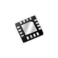
PCF2123BS/1,512 NXP Semiconductors, PCF2123BS/1,512 Datasheet - Page 36

PCF2123BS/1,512
Manufacturer Part Number
PCF2123BS/1,512
Description
IC CLOCK HVQFN16
Manufacturer
NXP Semiconductors
Type
Clock/Calendar/Alarmr
Datasheet
1.PCF2123TS1118.pdf
(61 pages)
Specifications of PCF2123BS/1,512
Package / Case
16-VQFN Exposed Pad, 16-HVQFN, 16-SQFN, 16-DHVQFN
Time Format
HH:MM:SS (12/24 hr)
Date Format
YY-MM-DD-dd
Interface
SPI, 3-Wire Serial
Voltage - Supply
1.1 V ~ 5.5 V
Operating Temperature
-40°C ~ 85°C
Mounting Type
Surface Mount
Function
Clock, Calendar, Alarm, Watchdog
Supply Voltage (max)
5.5 V
Supply Voltage (min)
1.1 V
Maximum Operating Temperature
+ 85 C
Minimum Operating Temperature
- 40 C
Mounting Style
SMD/SMT
Rtc Bus Interface
SPI
Supply Current
250 uA
Lead Free Status / RoHS Status
Lead free / RoHS Compliant
Memory Size
-
Lead Free Status / RoHS Status
Lead free / RoHS Compliant, Lead free / RoHS Compliant
Other names
568-5051-5
935286382512
935286382512
NXP Semiconductors
PCF2123
Product data sheet
8.12 3-line serial interface
Data transfer to and from the device is made via a 3-wire SPI-bus (see
data lines for input and output are split. The data input and output lines can be connected
together to facilitate a bidirectional data bus. The chip enable signal is used to identify the
transmitted data. Each data transfer is a byte, with the Most Significant Bit (MSB) sent first
(see
Table 41.
The transmission is controlled by the active HIGH chip enable signal CE. The first byte
transmitted is the command byte. Subsequent bytes will be either data to be written or
data to be read. Data is sampled on the rising edge of the clock and transferred internally
on the falling edge.
The command byte defines the address of the first register to be accessed and the
read/write mode. The address counter will auto increment after every access and will
rollover to zero after the last register is accessed. The read/write bit (R/W) defines if the
following bytes will be read or write information.
Symbol
CE
SCL
SDI
SDO
Fig 22. SDI, SDO configurations
Fig 23. Data transfer overview
Figure
Function
chip enable input
serial clock input
serial data input
serial data output
Serial interface
chip enable
23).
data bus
All information provided in this document is subject to legal disclaimers.
Rev. 4 — 22 December 2010
COMMAND
two wire mode
SDO
SDI
Description
when LOW, the interface is reset; pull-down resistor
included; active input may be higher than V
be wired permanently HIGH
when CE is LOW, this input may float; input may be higher
than V
when CE is LOW, input may float; input may be higher than
V
push-pull output; drives from V
changed on the falling edge of SCL; will be high-Z when not
driving; may be connected directly to SDI
DD
; input data is sampled on the rising edge of SCL
DATA
DD
single wire mode
SDO
SDI
DATA
001aai560
SPI Real time clock/calendar
SS
to V
DATA
DD
; output data is
PCF2123
© NXP B.V. 2010. All rights reserved.
Table
001aaf914
DD
, but may not
41). The
36 of 61


