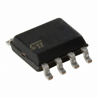
M41T56M6E STMicroelectronics, M41T56M6E Datasheet - Page 12

M41T56M6E
Manufacturer Part Number
M41T56M6E
Description
IC SRAM SRL TIMEKPR 512BIT 8SOIC
Manufacturer
STMicroelectronics
Type
Clock/Calendar/NVSRAMr
Specifications of M41T56M6E
Memory Size
56B
Time Format
HH:MM:SS (24 hr)
Date Format
YY-MM-DD-dd
Interface
I²C, 2-Wire Serial
Voltage - Supply
4.5 V ~ 5.5 V
Operating Temperature
-40°C ~ 85°C
Mounting Type
Surface Mount
Package / Case
8-SOIC (3.9mm Width)
Function
Clock/Calendar
Rtc Memory Size
64 Byte
Supply Voltage (max)
5.5 V
Supply Voltage (min)
4.5 V
Maximum Operating Temperature
+ 85 C
Minimum Operating Temperature
- 40 C
Mounting Style
SMD/SMT
Rtc Bus Interface
Serial (2-Wire, I2C)
Nvram Features
RTC, Internal Battery, XTAL
Interface Type
I2C, Serial, 2-Wire
Supply Voltage Range
4.5V To 5.5V
Memory Case Style
SOIC
No. Of Pins
8
Rohs Compliant
Yes
Lead Free Status / RoHS Status
Contains lead / RoHS non-compliant
Other names
497-2818-5
M41T56M6
M41T56M6
Available stocks
Company
Part Number
Manufacturer
Quantity
Price
Part Number:
M41T56M6E
Manufacturer:
ST
Quantity:
20 000
2.3
2.4
12/25
Write mode
In this mode the master transmitter transmits to the M41T56 slave receiver. Bus protocol is
shown in
(R/W = 0) is placed on the bus and indicates to the addressed device that word address A
will follow and is to be written to the on-chip address pointer. The data word to be written to
the memory is strobed in next and the internal address pointer is incremented to the next
memory location within the RAM on the reception of an acknowledge clock. The M41T56
slave receiver will send an acknowledge clock to the master transmitter after it has received
the slave address and again after it has received the word address and each data byte (see
Figure 7 on page
Data retention mode
With valid V
WRITE cycles. Should the supply voltage decay, the M41T56 will automatically deselect,
write protecting itself when V
accomplished by internally inhibiting access to the clock registers and SRAM.
falls below the Battery Back-up Switchover Voltage (V
V
battery supply.
All outputs become high impedance. On power up, when V
write protection continues for t
For a further more detailed review of battery lifetime calculations, please see Application
Note AN1012.
Figure 10. Write mode sequence
CC
pin to the battery and the clock registers and SRAM are maintained from the attached
BUS ACTIVITY:
MASTER
SDA LINE
BUS ACTIVITY:
Figure 10 on page
CC
applied, the M41T56 can be accessed as described above with READ or
11).
S
ADDRESS
SLAVE
12. Following the START condition and slave address, a logic '0'
CC
REC
falls between V
.
ADDRESS (n)
WORD
PFD
DATA n
(max) and V
SO
), power input is switched from the
CC
DATA n+1
returns to a nominal value,
PFD
(min). This is
DATA n+X
When V
AI00591
P
CC
n


