AD7760BSVZ Analog Devices Inc, AD7760BSVZ Datasheet - Page 10
AD7760BSVZ
Manufacturer Part Number
AD7760BSVZ
Description
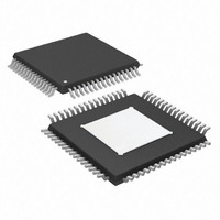
IC ADC 24BIT 2.5MSPS 64TQFP
Manufacturer
Analog Devices Inc
Datasheet
1.AD7760BSVZ.pdf
(36 pages)
Specifications of AD7760BSVZ
Data Interface
Parallel
Number Of Bits
24
Sampling Rate (per Second)
2.5M
Number Of Converters
1
Power Dissipation (max)
958mW
Voltage Supply Source
Analog and Digital
Operating Temperature
-40°C ~ 85°C
Mounting Type
Surface Mount
Package / Case
64-TQFP Exposed Pad
Resolution (bits)
24bit
Sampling Rate
2.5MSPS
Input Channel Type
Differential
Supply Voltage Range - Digital
2.375V To 2.625V
Supply Current
49mA
Lead Free Status / RoHS Status
Lead free / RoHS Compliant
Available stocks
Company
Part Number
Manufacturer
Quantity
Price
Company:

Part Number:
AD7760BSVZ
Manufacturer:
Analog Devices Inc
Quantity:
10 000
Part Number:
AD7760BSVZ
Manufacturer:
ADI/亚德诺
Quantity:
20 000
Company:
Part Number:
AD7760BSVZ-REEL
Manufacturer:
Analog Devices Inc
Quantity:
10 000


AD7760
Pin No.
30
17
45 to 52,
54 to 61
37
3
2
36
39
38
40
Mnemonic
DECAPB
R
DB15:DB8,
DB7:DB0
RESET
MCLK
MCLKGND
SYNC
RD/WR
DRDY
CS
BIAS
Description
Decoupling Pin. A 33 pF capacitor must be inserted between this pin and AGND3.
Bias Current Setting Pin. A resistor must be inserted between this pin and AGND. For more details, see the
Bias Resistor Selection section.
16-Bit Bidirectional Data Bus. These are three-state pins that are controlled by the CS pin and the RD/WR
pin. The operating voltage for these pins is determined by the V
Output Mode and AD7760 Interface sections for more details.
A falling edge on this pin resets all internal digital circuitry and powers down the part. Holding this pin low
keeps the AD7760 in a reset state.
Master Clock Input. A low jitter, buffered digital clock must be applied to this pin. The output data rate
depends on the frequency of this clock. See the Clocking the AD7760 section for more details.
Master Clock Ground Sensing Pin.
Synchronization Input. A falling edge on this pin resets the internal filter. This can be used to synchronize
multiple devices in a system. See the Synchronization section for more details.
Read/Write Input. This pin, in conjunction with the chip select pin, is used to read and write data to and
from the AD7760. If this pin is low when CS is low, a read takes place. If this pin is high when CS is low, a
write occurs. See the Modulator Data Output Mode and AD7760 Interface sections for more details.
Data Ready Output. Each time new conversion data is available, an active low pulse, ½ ICLK period wide, is
produced on this pin. See the Modulator Data Output Mode and AD7760 Interface sections for more details.
Chip Select Input. Used in conjunction with the RD/WR pin to read and write data from and to the AD7760.
See the Modulator Data Output Mode and AD7760 Interface sections for more details.
Rev. A | Page 10 of 36
DRIVE
voltage. See the Modulator Data
Related parts for AD7760BSVZ
Image
Part Number
Description
Manufacturer
Datasheet
Request
R

Part Number:
Description:
±1.7g Dual-Axis IMEMS Accelerometer Evaluation Board
Manufacturer:
Analog Devices Inc
Datasheet:

Part Number:
Description:
Inertial Sensor Evaluation System
Manufacturer:
Analog Devices Inc
Datasheet:
Part Number:
Description:
Manufacturer:
Analog Devices Inc
Datasheet:
Part Number:
Description:
Manufacturer:
Analog Devices Inc
Datasheet:
Part Number:
Description:
Manufacturer:
Analog Devices Inc
Datasheet:
Part Number:
Description:
Manufacturer:
Analog Devices Inc
Datasheet:
Part Number:
Description:
Manufacturer:
Analog Devices Inc
Datasheet:
Part Number:
Description:
Manufacturer:
Analog Devices Inc
Datasheet:
Part Number:
Description:
Manufacturer:
Analog Devices Inc
Datasheet:
Part Number:
Description:
Manufacturer:
Analog Devices Inc
Datasheet:
Part Number:
Description:
Manufacturer:
Analog Devices Inc
Datasheet:
Part Number:
Description:
Manufacturer:
Analog Devices Inc
Datasheet:
Part Number:
Description:
Manufacturer:
Analog Devices Inc
Datasheet: