AD7760BSVZ Analog Devices Inc, AD7760BSVZ Datasheet - Page 2
AD7760BSVZ
Manufacturer Part Number
AD7760BSVZ
Description
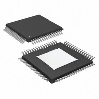
IC ADC 24BIT 2.5MSPS 64TQFP
Manufacturer
Analog Devices Inc
Datasheet
1.AD7760BSVZ.pdf
(36 pages)
Specifications of AD7760BSVZ
Data Interface
Parallel
Number Of Bits
24
Sampling Rate (per Second)
2.5M
Number Of Converters
1
Power Dissipation (max)
958mW
Voltage Supply Source
Analog and Digital
Operating Temperature
-40°C ~ 85°C
Mounting Type
Surface Mount
Package / Case
64-TQFP Exposed Pad
Resolution (bits)
24bit
Sampling Rate
2.5MSPS
Input Channel Type
Differential
Supply Voltage Range - Digital
2.375V To 2.625V
Supply Current
49mA
Lead Free Status / RoHS Status
Lead free / RoHS Compliant
Available stocks
Company
Part Number
Manufacturer
Quantity
Price
Company:

Part Number:
AD7760BSVZ
Manufacturer:
Analog Devices Inc
Quantity:
10 000
Part Number:
AD7760BSVZ
Manufacturer:
ADI/亚德诺
Quantity:
20 000
Company:
Part Number:
AD7760BSVZ-REEL
Manufacturer:
Analog Devices Inc
Quantity:
10 000


AD7760
TABLE OF CONTENTS
Features .............................................................................................. 1
Applications....................................................................................... 1
Functional Block Diagram .............................................................. 1
General Description ......................................................................... 1
Revision History ............................................................................... 3
Specifications..................................................................................... 4
Absolute Maximum Ratings............................................................ 8
Pin Configuration and Function Descriptions............................. 9
Terminology .................................................................................... 11
Typical Performance Characteristics ........................................... 12
Theory of Operation ...................................................................... 18
Modulator Data Output Mode...................................................... 19
Modulator Data Output Mode Interface ..................................... 20
AD7760 Interface............................................................................ 22
Timing Specifications .................................................................. 6
Timing Diagrams.......................................................................... 7
ESD Caution.................................................................................. 8
Modulator Inputs........................................................................ 19
Modulator Data Output Scaling ............................................... 19
Clock Divide-by-1 Mode ( CDIV = 1) ..................................... 20
Clock Divide-by-2 Mode ( CDIV = 0) ..................................... 20
Using the AD7760 in Modulator Output Mode..................... 21
Reading Data............................................................................... 22
Reading Status and Other Registers......................................... 22
Sharing the Parallel Bus ............................................................. 22
Synchronization.......................................................................... 22
Rev. A | Page 2 of 36
Clocking the AD7760 .................................................................... 24
Driving the AD7760....................................................................... 26
Decoupling and Layout Recommendations................................ 28
Programmable FIR Filter............................................................... 30
Downloading a User-Defined Filter ............................................ 31
AD7760 Registers ........................................................................... 33
Outline Dimensions ....................................................................... 35
Writing to the AD7760 .............................................................. 23
Buffering the MCLK signal....................................................... 24
MCLK Jitter Requirements ....................................................... 24
Using the AD7760 ...................................................................... 27
Supply Decoupling ..................................................................... 29
Additional Decoupling .............................................................. 29
Reference Voltage Filtering ....................................................... 29
Differential Amplifier Components ........................................ 29
Bias Resistor Selection ............................................................... 29
Layout Considerations............................................................... 29
Exposed Paddle........................................................................... 29
Example Filter Download ......................................................... 31
Control Register 1—Address 0x0001 ...................................... 33
Control Register 2—Address 0x0002 ...................................... 33
Status Register (Read Only) ...................................................... 34
Offset Register—Address 0x0003............................................. 34
Gain Register—Address 0x0004............................................... 34
Overrange Register—Address 0x0005..................................... 34
Ordering Guide .......................................................................... 35
Related parts for AD7760BSVZ
Image
Part Number
Description
Manufacturer
Datasheet
Request
R

Part Number:
Description:
±1.7g Dual-Axis IMEMS Accelerometer Evaluation Board
Manufacturer:
Analog Devices Inc
Datasheet:

Part Number:
Description:
Inertial Sensor Evaluation System
Manufacturer:
Analog Devices Inc
Datasheet:
Part Number:
Description:
Manufacturer:
Analog Devices Inc
Datasheet:
Part Number:
Description:
Manufacturer:
Analog Devices Inc
Datasheet:
Part Number:
Description:
Manufacturer:
Analog Devices Inc
Datasheet:
Part Number:
Description:
Manufacturer:
Analog Devices Inc
Datasheet:
Part Number:
Description:
Manufacturer:
Analog Devices Inc
Datasheet:
Part Number:
Description:
Manufacturer:
Analog Devices Inc
Datasheet:
Part Number:
Description:
Manufacturer:
Analog Devices Inc
Datasheet:
Part Number:
Description:
Manufacturer:
Analog Devices Inc
Datasheet:
Part Number:
Description:
Manufacturer:
Analog Devices Inc
Datasheet:
Part Number:
Description:
Manufacturer:
Analog Devices Inc
Datasheet:
Part Number:
Description:
Manufacturer:
Analog Devices Inc
Datasheet: