AD7760BSVZ Analog Devices Inc, AD7760BSVZ Datasheet - Page 29
AD7760BSVZ
Manufacturer Part Number
AD7760BSVZ
Description
IC ADC 24BIT 2.5MSPS 64TQFP
Manufacturer
Analog Devices Inc
Datasheet
1.AD7760BSVZ.pdf
(36 pages)
Specifications of AD7760BSVZ
Data Interface
Parallel
Number Of Bits
24
Sampling Rate (per Second)
2.5M
Number Of Converters
1
Power Dissipation (max)
958mW
Voltage Supply Source
Analog and Digital
Operating Temperature
-40°C ~ 85°C
Mounting Type
Surface Mount
Package / Case
64-TQFP Exposed Pad
Resolution (bits)
24bit
Sampling Rate
2.5MSPS
Input Channel Type
Differential
Supply Voltage Range - Digital
2.375V To 2.625V
Supply Current
49mA
Lead Free Status / RoHS Status
Lead free / RoHS Compliant
Available stocks
Company
Part Number
Manufacturer
Quantity
Price
Company:

Part Number:
AD7760BSVZ
Manufacturer:
Analog Devices Inc
Quantity:
10 000
Part Number:
AD7760BSVZ
Manufacturer:
ADI/亚德诺
Quantity:
20 000
Company:
Part Number:
AD7760BSVZ-REEL
Manufacturer:
Analog Devices Inc
Quantity:
10 000


SUPPLY DECOUPLING
Every supply pin must be connected to the appropriate supply
via a ferrite bead and decoupled to the correct ground pin with
a 100 nF, 0603 case size, X7R dielectric capacitor. There are two
exceptions to this:
ADDITIONAL DECOUPLING
There are two other decoupling pins on the AD7760—Pin 8
(DECAPA) and Pin 30 (DECAPB). Pin 8 should be decoupled
with a 100 nF capacitor, and Pin 30 requires a 33 pF capacitor.
REFERENCE VOLTAGE FILTERING
A low noise reference source, such as the
ADR434
reference voltage supplied to the AD7760 should be decoupled
and filtered as shown in Figure 56.
The recommended scheme for the reference voltage supply is a
100 Ω series resistor connected to a 100 μF tantalum capacitor,
followed by a series resistor of 10 Ω, and finally a 10 nF capacitor
placed as close as possible to the V
capacitor to the associated ground pin, Pin 11.
7.5V
DIFFERENTIAL AMPLIFIER COMPONENTS
The correct components for use around the on-chip differential
amplifier are detailed in Table 8. Matching the components on
both sides of the differential amplifier is important to minimize
distortion of the signal applied to the amplifier. A tolerance of
0.1% or better is required for these components. Symmetrical
routing of the tracks on both sides of the differential amplifier
also assists in achieving the stated performance.
•
•
Pin 12 (AV
the pin and a 10 nF decoupling capacitor, which is
connected to ground at Pin 9.
Pin 27 (AV
capacitor or a direct connection to the supply, but instead
is connected to Pin 14 via a 15 nH inductor.
10µF
C15
(4.096 V), is suitable for use with the AD7760. The
+
100nF
C9
DD
DD
4) must have a 10 Ω resistor inserted between
2) does not require a separate decoupling
Figure 56. Reference Connection
2
V
IN
ADR434
GND
4
U3
V
OUT
6
REF+
100Ω
R30
100µF
pin, decoupling this
C11
ADR431
+
10nF
R17
10Ω
C46
(2.5 V) or
PIN 10
Rev. A | Page 29 of 36
BIAS RESISTOR SELECTION
The AD7760 requires a resistor to be connected between the
R
on the reference voltage being applied to the device. The resistor
value should be selected to produce a current of 25 μA through
the resistor to ground. For a 2.5 V reference voltage, the correct
resistor value is 100 kΩ, and for a 4.096 V reference, the correct
resistor value is 160 kΩ.
LAYOUT CONSIDERATIONS
While using the correct components is essential to achieve
optimum performance, the correct layout is just as important.
The
contains the Gerber files for the AD7760 evaluation board.
These files should be used as a reference when designing any
system using the AD7760.
The location and orientation of some of the components
mentioned in previous sections of this data sheet are critical,
and particular attention must be paid to the components that
are located close to the AD7760. Locating these components
farther away from the device can have a direct impact on the
achievable maximum performance.
The use of ground planes should also be carefully considered.
To ensure that the return currents through the decoupling
capacitors are flowing to the correct ground pin, the ground side
of the capacitors should be as close as possible to the ground pin
associated with that supply. A ground plane should not be relied
on as the sole return path for decoupling capacitors because the
return current path using ground planes is not easily predictable.
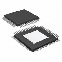
EXPOSED PADDLE
The AD7760 64-lead TQFP employs a 6 mm × 6 mm exposed
paddle (see Figure 59). The paddle reduces the thermal
resistance of the package by providing a path for heat energy to
flow between the package and the PCB and, in turn, increases
the heat transfer efficiency from the AD7760 package.
Connecting the exposed paddle to the AGND plane of the PCB
is essential in creating the conditions that allow the AD7760
package to perform to the highest specifications possible. The
exposed paddle should not be connected directly to any of the
ground pins on the AD7760 and should only be connected to
the analog ground plane. Best practice is to use multiple vias
connecting the exposed paddle to the AGND plane of the PCB.
BIAS
AD7760 product page
and AGND pins. The value of this resistor is dependent
on the Analog Devices website
AD7760
Related parts for AD7760BSVZ
Image
Part Number
Description
Manufacturer
Datasheet
Request
R

Part Number:
Description:
±1.7g Dual-Axis IMEMS Accelerometer Evaluation Board
Manufacturer:
Analog Devices Inc
Datasheet:

Part Number:
Description:
Inertial Sensor Evaluation System
Manufacturer:
Analog Devices Inc
Datasheet:
Part Number:
Description:
Manufacturer:
Analog Devices Inc
Datasheet:
Part Number:
Description:
Manufacturer:
Analog Devices Inc
Datasheet:
Part Number:
Description:
Manufacturer:
Analog Devices Inc
Datasheet:
Part Number:
Description:
Manufacturer:
Analog Devices Inc
Datasheet:
Part Number:
Description:
Manufacturer:
Analog Devices Inc
Datasheet:
Part Number:
Description:
Manufacturer:
Analog Devices Inc
Datasheet:
Part Number:
Description:
Manufacturer:
Analog Devices Inc
Datasheet:
Part Number:
Description:
Manufacturer:
Analog Devices Inc
Datasheet:
Part Number:
Description:
Manufacturer:
Analog Devices Inc
Datasheet:
Part Number:
Description:
Manufacturer:
Analog Devices Inc
Datasheet:
Part Number:
Description:
Manufacturer:
Analog Devices Inc
Datasheet: