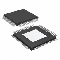
AD7760BSVZ Analog Devices Inc, AD7760BSVZ Datasheet - Page 21

AD7760BSVZ
Manufacturer Part Number
AD7760BSVZ
Description
IC ADC 24BIT 2.5MSPS 64TQFP
Manufacturer
Analog Devices Inc
Datasheet
1.AD7760BSVZ.pdf
(36 pages)
Specifications of AD7760BSVZ
Data Interface
Parallel
Number Of Bits
24
Sampling Rate (per Second)
2.5M
Number Of Converters
1
Power Dissipation (max)
958mW
Voltage Supply Source
Analog and Digital
Operating Temperature
-40°C ~ 85°C
Mounting Type
Surface Mount
Package / Case
64-TQFP Exposed Pad
Resolution (bits)
24bit
Sampling Rate
2.5MSPS
Input Channel Type
Differential
Supply Voltage Range - Digital
2.375V To 2.625V
Supply Current
49mA
Lead Free Status / RoHS Status
Lead free / RoHS Compliant
Available stocks
Company
Part Number
Manufacturer
Quantity
Price
Company:
Part Number:
AD7760BSVZ
Manufacturer:
Analog Devices Inc
Quantity:
10 000
Part Number:
AD7760BSVZ
Manufacturer:
ADI/亚德诺
Quantity:
20 000
Company:
Part Number:
AD7760BSVZ-REEL
Manufacturer:
Analog Devices Inc
Quantity:
10 000
In the case where n is an odd number of MCLK cycles, the
modulator data output on Pins D [15:0] is output on the rising
edge of DRDY . In this case, the modulator data should be read
on the falling edge of MCLK when DRDY is logic low. Figure 45
shows timing details to be used when reading the modulator
output data where CDIV = 0 and there is an odd number of
MCLK cycles between the rising edge of RESET and the rising
edge of SYNC . The edge of MCLK that should be used under
these conditions is illustrated in Figure 45 by arrows on the
MCLK falling edges in question.
USING THE AD7760
IN MODULATOR OUTPUT MODE
The following is the recommended sequence for powering up
and using the AD7760:
1.
2.
3.
4.
Apply power.
Start the clock oscillator, applying MCLK.
Take RESET low for a minimum of one MCLK cycle.
Wait a minimum of two MCLK cycles after the rising edge
of RESET .
CS, RD/WR
D[0:15]
MCLK
DRDY
t
11
INVALID DATA
Figure 45. AD7760 Modulator Output Mode ( CDIV = 0, n is odd)
Rev. A | Page 21 of 36
t
9
MOD DATA M
t
19
t
20
Using this sequence results in an even number of MCLK cycles
between the rising edge of RESET and the rising edge of SYNC .
Therefore, when using this sequence with CDIV = 0, the interface
timing shown in Figure 43 should be implemented.
Note that whether the number of MCLK cycles between the
rising edge of RESET and SYNC is odd or even is irrelevant
when the AD7760 is operated with CDIV = 1.
When using the AD7760 in modulator output mode, the offset,
gain, and overrange registers are not operational. The only
registers that can be used are Control Register 1 and Control
Register 2.
5.
6.
7.
8.
t
10
Write to Control Register 2 to power up the ADC and the
differential amplifier as required. The correct clock divider
( CDIV ) ratio should be programmed at this time.
Write to Control Register 1 to set the bypass filter bits, BYP F1
and BYP F3 , and the decimation rate bits, DEC [2:0], to 0.
Wait a minimum of six MCLK cycles after the rising edge
of CS has been released.
Take SYNC low for a minimum of four MCLK cycles, if
required, to synchronize multiple parts.
MOD DATA M + 1
MOD D...
t
14
AD7760


