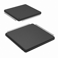
ADC08D500CIYB/NOPB National Semiconductor, ADC08D500CIYB/NOPB Datasheet

ADC08D500CIYB/NOPB
Manufacturer Part Number
ADC08D500CIYB/NOPB
Description
IC ADC 8BIT 500MSPS DUAL 128LQFP
Manufacturer
National Semiconductor
Series
PowerWise®r
Specifications of ADC08D500CIYB/NOPB
Number Of Bits
8
Sampling Rate (per Second)
500M
Data Interface
Serial
Number Of Converters
2
Power Dissipation (max)
1.78W
Voltage Supply Source
Single Supply
Operating Temperature
-40°C ~ 85°C
Mounting Type
Surface Mount
Package / Case
128-LQFP Exposed Pad
Lead Free Status / RoHS Status
Lead free / RoHS Compliant
Other names
*ADC08D500CIYB
*ADC08D500CIYB/NOPB
ADC08D500CIYB
*ADC08D500CIYB/NOPB
ADC08D500CIYB
Available stocks
Company
Part Number
Manufacturer
Quantity
Price
Company:
Part Number:
ADC08D500CIYB/NOPB
Manufacturer:
Texas Instruments
Quantity:
10 000
© 2005 National Semiconductor Corporation
ADC08D500
High Performance, Low Power, Dual 8-Bit, 500 MSPS A/D
Converter
General Description
The ADC08D500 is a dual, low power, high performance
CMOS analog-to-digital converter that digitizes signals to 8
bits resolution at sampling rates up to 800 MSPS. Consum-
ing a typical 1.4 Watts at 500 MSPS from a single 1.9 Volt
supply, this device is guaranteed to have no missing codes
over the full operating temperature range. The unique folding
and interpolating architecture, the fully differential compara-
tor design, the innovative design of the internal sample-and-
hold amplifier and the self-calibration scheme enable a very
flat response of all dynamic parameters beyond Nyquist,
producing a high 7.5 ENOB with a 250 MHz input signal and
a 500 MHz sample rate while providing a 10
formatting is offset binary and the LVDS digital outputs are
compliant with IEEE 1596.3-1996, with the exception of an
adjustable common mode voltage between 0.8V and 1.2V.
Each converter has a 1:2 demultiplexer that feeds two LVDS
buses and reduces the output data rate on each bus to half
the sampling rate. The two converters can be interleaved
and used as a single 1 GSPS ADC.
The converter typically consumes less than 3.5 mW in the
Power Down Mode and is available in a 128-lead, thermally
enhanced exposed pad LQFP and operates over the Indus-
trial (-40˚C ≤ T
Block Diagram
A
≤ +85˚C) temperature range.
DS201214
-18
B.E.R. Output
Features
n Internal Sample-and-Hold
n Single +1.9V
n Choice of SDR or DDR output clocking
n Interleave Mode for 2x Sampling Rate
n Multiple ADC Synchronization Capability
n Guaranteed No Missing Codes
n Serial Interface for Extended Control
n Fine Adjustment of Input Full-Scale Range and Offset
n Duty Cycle Corrected Sample Clock
Key Specifications
n Resolution
n Max Conversion Rate
n Bit Error Rate
n ENOB
n DNL
n Power Consumption
Applications
n Direct RF Down Conversion
n Digital Oscilloscopes
n Satellite Set-top boxes
n Communications Systems
n Test Instrumentation
— Operating
— Power Down Mode
@
250 MHz Input
±
0.1V Operation
20121453
500 MSPS (min)
December 2005
±
0.15 LSB (typ)
www.national.com
3.5 mW (typ)
7.5 Bits (typ)
1.4 W (typ)
10
-18
8 Bits
(typ)


