ADC08D500CIYB/NOPB National Semiconductor, ADC08D500CIYB/NOPB Datasheet - Page 4
ADC08D500CIYB/NOPB
Manufacturer Part Number
ADC08D500CIYB/NOPB
Description
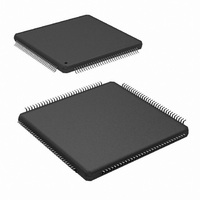
IC ADC 8BIT 500MSPS DUAL 128LQFP
Manufacturer
National Semiconductor
Series
PowerWise®r
Specifications of ADC08D500CIYB/NOPB
Number Of Bits
8
Sampling Rate (per Second)
500M
Data Interface
Serial
Number Of Converters
2
Power Dissipation (max)
1.78W
Voltage Supply Source
Single Supply
Operating Temperature
-40°C ~ 85°C
Mounting Type
Surface Mount
Package / Case
128-LQFP Exposed Pad
Lead Free Status / RoHS Status
Lead free / RoHS Compliant
Other names
*ADC08D500CIYB
*ADC08D500CIYB/NOPB
ADC08D500CIYB
*ADC08D500CIYB/NOPB
ADC08D500CIYB
Available stocks
Company
Part Number
Manufacturer
Quantity
Price
Company:

Part Number:
ADC08D500CIYB/NOPB
Manufacturer:
Texas Instruments
Quantity:
10 000


www.national.com
Pin Functions
Pin No.
Pin Descriptions and Equivalent Circuits
126
18
19
11
10
22
23
31
32
34
35
7
.
Tdiode_P
Tdiode_N
Symbol
CalRun
V
V
CLK+
V
CLK-
V
V
R
V
IN
IN
CMO
IN
IN
EXT
BG
.
Q+
Q−
I+
I−
Equivalent Circuit
4
LVDS Clock input pins for the ADC. The differential clock
signal must be a.c. coupled to these pins. The input signal is
sampled on the falling edge of CLK+. See Section 1.1.2 for a
description of acquiring the input and Section 2.3 for an
overview of the clock inputs.
Analog signal inputs to the ADC. The differential full-scale
input range is 650 mV
mV
Common Mode Voltage. The voltage output at this pin is
required to be the common mode input voltage at V
V
when a.c. coupling is used at the analog inputs. This pin is
capable of sourcing or sinking 100µA. See Section 2.2.
Bandgap output voltage capable of 100 µA source/sink.
Calibration Running indication. This pin is at a logic high when
calibration is running.
External bias resistor connection. Nominal value is 3.3k-Ohms
(
Temperature Diode Positive (Anode) and Negative (Cathode)
for die temperature measurements. See Section 2.6.2.
±
IN
0.1%) to ground. See Section 1.1.1.
P-P
− when d.c. coupling is used. This pin should be grounded
(Continued)
when the FSR pin is high.
P-P
Description
when the FSR pin is low, or 870
IN
+ and
Related parts for ADC08D500CIYB/NOPB
Image
Part Number
Description
Manufacturer
Datasheet
Request
R

Part Number:
Description:
National Semiconductor [8-Bit D/A Converter]
Manufacturer:
National Semiconductor
Datasheet:
Part Number:
Description:
National Semiconductor [Media Coprocessor]
Manufacturer:
National Semiconductor
Datasheet:
Part Number:
Description:
Digitally Controlled Tone and Volume Circuit with Stereo Audio Power Amplifier, Microphone Preamp Stage and National 3D Sound
Manufacturer:
National Semiconductor
Datasheet:
Part Number:
Description:
Digitally Controlled Tone and Volume Circuit with Stereo Audio Power Amplifier, Microphone Preamp Stage and National 3D Sound
Manufacturer:
National Semiconductor
Datasheet:
Part Number:
Description:
AC97 Rev 2 Codec with Sample Rate Conversion and National 3D Sound
Manufacturer:
National Semiconductor
Part Number:
Description:
Manufacturer:
National Semiconductor
Datasheet:
Part Number:
Description:
Manufacturer:
National Semiconductor
Datasheet:
Part Number:
Description:
General Purpose, Low Voltage, Low Power, Rail-to-Rail Output Operational Amplifiers
Manufacturer:
National Semiconductor
Datasheet:
Part Number:
Description:
8-bit 20 MSPS flash A/D converter.
Manufacturer:
National Semiconductor
Datasheet:
Part Number:
Description:
Low Noise Quad Operational Amplifier
Manufacturer:
National Semiconductor
Datasheet:
Part Number:
Description:
Quad Differential Line Receivers
Manufacturer:
National Semiconductor
Datasheet:
Part Number:
Description:
Quad High Speed Trapezoidal? Bus Transceiver
Manufacturer:
National Semiconductor
Datasheet:
Part Number:
Description:
Dual Line Receiver
Manufacturer:
National Semiconductor
Datasheet:
Part Number:
Description:
TTL to 10k ECL Level Translator with Latch
Manufacturer:
National Semiconductor
Datasheet: