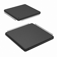
ADC08D500CIYB/NOPB National Semiconductor, ADC08D500CIYB/NOPB Datasheet - Page 5

ADC08D500CIYB/NOPB
Manufacturer Part Number
ADC08D500CIYB/NOPB
Description
IC ADC 8BIT 500MSPS DUAL 128LQFP
Manufacturer
National Semiconductor
Series
PowerWise®r
Specifications of ADC08D500CIYB/NOPB
Number Of Bits
8
Sampling Rate (per Second)
500M
Data Interface
Serial
Number Of Converters
2
Power Dissipation (max)
1.78W
Voltage Supply Source
Single Supply
Operating Temperature
-40°C ~ 85°C
Mounting Type
Surface Mount
Package / Case
128-LQFP Exposed Pad
Lead Free Status / RoHS Status
Lead free / RoHS Compliant
Other names
*ADC08D500CIYB
*ADC08D500CIYB/NOPB
ADC08D500CIYB
*ADC08D500CIYB/NOPB
ADC08D500CIYB
Available stocks
Company
Part Number
Manufacturer
Quantity
Price
Company:
Part Number:
ADC08D500CIYB/NOPB
Manufacturer:
Texas Instruments
Quantity:
10 000
Pin Functions
100 / 61
101 / 60
102 / 59
103 / 58
104 / 57
105 / 56
106 / 55
107 / 54
111 / 50
112 / 49
113 / 48
114 / 47
115 / 46
116 / 45
117 / 44
118 / 43
122 / 39
123 / 38
124 / 37
125 / 36
Pin No.
33, 128
83 / 78
84 / 77
85 / 76
86 / 75
89 / 72
90 / 71
91 / 70
92 / 69
93 / 68
94 / 67
95 / 66
96 / 65
2, 5, 8,
Pin Descriptions and Equivalent Circuits
13, 16,
17, 20,
25, 28,
79
80
82
81
DId7− / DQd7−
DId7+ / DQd7+
DId6− / DQd6−
DId6+ / DQd6+
DId5− / DQd5−
DId5+ / DQd5+
DId4− / DQd4−
DId4+ / DQd4+
DId3− / DQd3−
DId3+ / DQd3+
DId2− / DQd2−
DId2+ / DQd2+
DId1− / DQd1−
DId1+ / DQd1+
DId0− / DQd0−
DId0+ / DQd0+
DI7− / DQ7−
DI7+ / DQ7+
DI6− / DQ6−
DI6+ / DQ6+
DI5− / DQ5−
DI5+ / DQ5+
DI4− / DQ4−
DI4+ / DQ4+
DI3− / DQ3−
DI3+ / DQ3+
DI2− / DQ2−
DI2+ / DQ2+
DI1− / DQ1−
DI1+ / DQ1+
DI0− / DQ0−
DI0+ / DQ0+
Symbol
DCLK+
DCLK-
OR+
OR-
V
A
Equivalent Circuit
5
I and Q channel LVDS Data Outputs that are not delayed in
the output demultiplexer. Compared with the DId and DQd
outputs, these outputs represent the later time samples.
These outputs should always be terminated with a 100Ω
differential resistor.
I and Q channel LVDS Data Outputs that are delayed by one
CLK cycle in the output demultiplexer. Compared with the
DI/DQ outputs, these outputs represent the earlier time
sample. These outputs should always be terminated with a
100Ω differential resistor.
Out Of Range output. A differential high at these pins
indicates that the differential input is out of range (outside the
range
Differential Clock outputs used to latch the output data.
Delayed and non-delayed data outputs are supplied
synchronous to this signal. This signal is at 1/2 the input clock
rate in SDR mode and at 1/4 the input clock rate in the DDR
mode.
Analog power supply pins. Bypass these pins to ground.
(Continued)
±
325 mV or
±
435 mV as defined by the FSR pin).
Description
www.national.com


