ADC083000CIYB/NOPB National Semiconductor, ADC083000CIYB/NOPB Datasheet
ADC083000CIYB/NOPB
Specifications of ADC083000CIYB/NOPB
*ADC083000CIYB/NOPB
ADC083000CIYB
Available stocks


Related parts for ADC083000CIYB/NOPB

ADC083000CIYB/NOPB Summary of contents
Page 1
... T +85°C) temperature range. A Ordering Information Industrial Temperature Range (-40°C < T ADC083000CIYB © 2009 National Semiconductor Corporation ADC083000 Features ■ Single +1.9V ±0.1V Operation ■ Choice of SDR or DDR output clocking ■ Serial Interface for Extended Control ■ ...
Page 2
Block Diagram www.national.com 2 20193253 ...
Page 3
Pin Configuration Note: The exposed pad on the bottom of the package must be soldered to a ground plane to ensure rated performance. 3 20193201 www.national.com ...
Page 4
Pin Descriptions and Equivalent Circuits Pin Functions Pin No. Symbol 3 OutV / SCLK OutEdge / DDR / 4 SDATA 15 DCLK_RST CAL 14 FSR/ECE www.national.com Equivalent Circuit Output Voltage Amplitude / Serial Interface Clock (Input):LVCMOS Tie ...
Page 5
Pin Functions Pin No. Symbol Equivalent Circuit 127 CalDly / SCS 10 CLK+ 11 CLK − DCLK_RST+ 23 DCLK_RST CMO Description Calibration Delay / Serial Interface Chip Select (Input):LVCMOS With ...
Page 6
Pin Functions Pin No. Symbol 126 CalRun R 32 EXT 34 Tdiode_P 35 Tdiode_N www.national.com Equivalent Circuit Bandgap Output Voltage (Output):Analog - Capable of 100 μA source/sink and can drive a load pF. Calibration ...
Page 7
Pin Functions Pin No. Symbol Equivalent Circuit Da0+ / Da0 Da1+ / Da1 Da2+ / Da2− Da3+ / Da3 Da4+ / Da4− ...
Page 8
Pin Functions Pin No. Symbol 13, 16, 17, 20 25, 28, 33, 128 40, 51 ,62, 73, 88, 99 110, 121 12, GND 21, 24, 27 42, 53, 64, 74, ...
Page 9
... Absolute Maximum Ratings (Notes Military/Aerospace specified devices are required, please contact the National Semiconductor Sales Office/ Distributors for availability and specifications. Supply Voltage ( Supply Difference Voltage on Any Input Pin (Except Voltage (Maintaining Common Mode) Ground Difference |GND - DR GND| Input Current at Any Pin (Note 3) Package Input Current (Note 3) ≤ ...
Page 10
Symbol Parameter Signal-to-Noise Plus Distortion SINAD Ratio SNR Signal-to-Noise Ratio THD Total Harmonic Distortion 2nd Harm Second Harmonic Distortion 3rd Harm Third Harmonic Distortion SFDR Spurious-Free dynamic Range IMD Intermodulation Distortion ANALOG INPUT AND REFERENCE CHARACTERISTICS Full Scale Analog Differential ...
Page 11
Symbol Parameter TEMPERATURE DIODE CHARACTERISTICS ΔV Temperature Diode Voltage BE LVDS INPUT CHARACTERISTICS V Differential Clock Input Level ID I Input Current I C Input Capacitance (Notes 10, 11) IN LVDS OUTPUT CHARACTERISTICS V LVDS Differential Output Voltage OD Change ...
Page 12
Symbol Parameter AC ELECTRICAL CHARACTERISTICS - Sampling Clock f Maximum Input Clock Frequency Sampling rate is 2x clock input CLK1 f Minimum Input Clock Frequency Sampling rate is 2x clock input CLK2 t Input Clock Duty Cycle CYC t Input ...
Page 13
Note 1: Absolute Maximum Ratings indicate limits beyond which damage to the device may occur. There is no guarantee of operation at the Absolute Maximum Ratings. Operating Ratings indicate conditions for which the device is functional, but do not guarantee ...
Page 14
ADC input at the same time defined as the ratio of the power in the second and third order intermodulation products to the power in one of the original frequencies. IMD is usually ...
Page 15
Transfer Characteristic FIGURE 2. Input / Output Transfer Characteristic 15 20193222 www.national.com ...
Page 16
Timing Diagrams www.national.com FIGURE 3. ADC083000 Timing — SDR Clocking FIGURE 4. ADC083000 Timing — DDR Clocking 16 20193214 20193259 ...
Page 17
FIGURE 5. Clock Reset Timing in DDR Mode FIGURE 6. Clock Reset Timing in SDR Mode with OUTEDGE Low FIGURE 7. Clock Reset Timing in SDR Mode with OUTEDGE High 17 20193220 20193223 20193224 www.national.com ...
Page 18
FIGURE 8. Calibration and On-Command Calibration Timing www.national.com FIGURE 9. Serial Interface Timing 18 20193225 20193219 ...
Page 19
Typical Performance Characteristics DNL vs. TEMPERATURE DNL vs. CODE POWER DISSIPATION vs. SAMPLE RATE V =V =1.9V, F =1500MHz CLK INL vs. TEMPERATURE 20193268 20193294 ENOB vs. TEMPERATURE 20193269 19 =25°C unless otherwise stated. A 20193293 INL ...
Page 20
ENOB vs. SUPPLY VOLTAGE ENOB vs. INPUT FREQUENCY SNR vs. SUPPLY VOLTAGE www.national.com ENOB vs. SAMPLE RATE 20193271 SNR vs. TEMPERATURE 20193273 SNR vs. SAMPLE RATE 20193275 20 20193272 20193274 20193276 ...
Page 21
SNR vs. INPUT FREQUENCY 20193277 THD vs. SUPPLY VOLTAGE 20193279 THD vs. INPUT FREQUENCY 20193281 THD vs. TEMPERATURE THD vs. SAMPLE RATE SFDR vs. TEMPERATURE 21 20193278 20193280 20193282 www.national.com ...
Page 22
SFDR vs. SUPPLY VOLTAGE SFDR vs. INPUT FREQUENCY Spectral Response at FIN = 748 MHz www.national.com SFDR vs. SAMPLE RATE 20193283 Spectral Response at FIN = 373 MHz 20193285 Spectral Response at FIN = 1497 MHz 20193287 22 20193284 20193296 ...
Page 23
FULL POWER BANDWIDTH 20193290 23 www.national.com ...
Page 24
Functional Description The ADC083000 is a versatile A/D Converter with an innova- tive architecture permitting very high speed operation. The controls available ease the application of the device to circuit solutions. Optimum performance requires adherence to the provisions discussed ...
Page 25
The ADC083000 will convert as long as the input clock signal is present. The fully differential comparator design and the innovative design of the sample-and-hold amplifier, together with calibration, enables very good SINAD/ENOB response beyond 1.5 GHz. The ADC083000 output ...
Page 26
higher common mode is required. A IMPORTANT NOTE: Tying the V BG crease the differential LVDS output voltage (V 40mV. 1.1.7 Power Down The ADC083000 is in ...
Page 27
The default state of the Extended Control Mode is set upon power-on reset (internally performed by the device) and is shown in Table 3. TABLE 3. Extended Control Mode Operation (Pin 14 Floating) Extended Control Mode Feature Default State SDR ...
Page 28
REGISTER DESCRIPTION Eight write-only registers provide several control and config- uration options in the Extended Control Mode. These regis- ters have no effect when the device is in the Normal Control Mode. Each register description below also shows the ...
Page 29
Full-Scale Voltage Adjust Addr: 3h (0011b) W only (0x807F) D15 D14 D13 D12 D11 D10 (MSB) Adjust Value (LSB Bit 15:7 Full Scale Voltage Adjust Value. The input full- ...
Page 30
Note Regarding Extended Mode Offset Correction When using the Offset Adjust register, the following informa- tion should be noted. For offset values of +0000 0000 and -0000 0000, the actual offset is not the same. By changing only the ...
Page 31
Applications Information 2.1 THE REFERENCE VOLTAGE The voltage reference for the ADC083000 is derived from a 1.254V bandgap reference, a buffered version of which is made available at pin 31 for user convenience. This BG output has ...
Page 32
When selecting a balun important to understand the input architecture of the ADC. There are specific balun parameters of which the ...
Page 33
FIGURE 14. Differential Sample Clock Connection The differential sample clock line pair should have a charac- teristic impedance of 100Ω and be terminated at the clock source in that (100Ω) characteristic impedance. The input clock line should be as ...
Page 34
Calibration The ADC083000 calibration must be run to achieve specified performance. The calibration procedure is run upon power-up and can be run any time on command. The calibration pro- cedure is exactly the same whether there is an input ...
Page 35
If the PD input is brought high while a calibration is running, the device will not go into power down until the calibration sequence is ...
Page 36
This is not a problem if the ambient temperature is kept to a maximum of +85°C as specified in the Operating Ratings section and the exposed pad on the bottom of the package is thermally connected to a ...
Page 37
Other signals can introduce jitter into the input clock signal. The clock signal can also in- troduce noise into the analog path if not isolated from that path. Best dynamic performance is obtained ...
Page 38
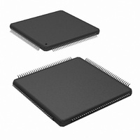
Physical Dimensions NOTES: UNLESS OTHERWISE SPECIFIED REFERENCE JEDEC REGISTRATION MS-026, VARIATION BFB. www.national.com inches (millimeters) unless otherwise noted 128-Lead Exposed Pad LQFP NS Package Number VNX128A 38 ...
Page 39
Notes 39 www.national.com ...
Page 40
... For more National Semiconductor product information and proven design tools, visit the following Web sites at: Products Amplifiers www.national.com/amplifiers Audio www.national.com/audio Clock and Timing www.national.com/timing Data Converters www.national.com/adc Interface www.national.com/interface LVDS www.national.com/lvds Power Management www.national.com/power Switching Regulators www.national.com/switchers LDOs www.national.com/ldo LED Lighting www ...