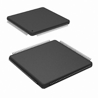
ADC083000CIYB/NOPB National Semiconductor, ADC083000CIYB/NOPB Datasheet - Page 5

ADC083000CIYB/NOPB
Manufacturer Part Number
ADC083000CIYB/NOPB
Description
IC ADC 8BIT 3GSPS LP 128-LQFP
Manufacturer
National Semiconductor
Series
PowerWise®r
Datasheet
1.ADC083000CIYBNOPB.pdf
(40 pages)
Specifications of ADC083000CIYB/NOPB
Number Of Bits
8
Sampling Rate (per Second)
3G
Data Interface
Serial
Number Of Converters
2
Power Dissipation (max)
2.3W
Voltage Supply Source
Single Supply
Operating Temperature
-40°C ~ 85°C
Mounting Type
Surface Mount
Package / Case
128-LQFP Exposed Pad
Lead Free Status / RoHS Status
Lead free / RoHS Compliant
Other names
*ADC083000CIYB
*ADC083000CIYB/NOPB
ADC083000CIYB
*ADC083000CIYB/NOPB
ADC083000CIYB
Available stocks
Company
Part Number
Manufacturer
Quantity
Price
Company:
Part Number:
ADC083000CIYB/NOPB
Manufacturer:
IPS
Quantity:
2 300
Part Number:
ADC083000CIYB/NOPB
Manufacturer:
TI/德州仪器
Quantity:
20 000
Pin Functions
Pin No.
127
10
11
18
19
22
23
7
CalDly / SCS
DCLK_RST+
DCLK_RST-
Symbol
CLK+
V
CLK-
V
V
CMO
IN
IN
+
−
Equivalent Circuit
5
Calibration Delay / Serial Interface Chip Select
(Input):LVCMOS With a logic high or low on pin 14, this pin
functions as Calibration Delay and sets the number of input clock
cycles after power up before calibration begins (See Section
1.1.1). With pin 14 floating, this pin acts as the enable pin for the
serial interface input and the CalDly value becomes "0" (short
delay with no provision for a long power-up calibration delay).
Sampling Clock Input
(Input):LVDS The differential clock signal must be a.c. coupled
to these pins. The input signal is sampled on both the rising and
falling edge of CLK. See Section 1.1.2 for a description of
acquiring the input and Section 2.3 for an overview of the clock
inputs.
Signal Input
(Input):Analog The differential full-scale input range is 600
mV
is high. In the Extended Control Mode, FSR is determined by the
Full-Scale Voltage Adjust register (address 3h, bits 15:7).
Sample Clock Reset
(Input):LVDS A positive differerntial pulse on these pins is used
to reset and synchronize the DCLK outs of multiple converters.
See Section 1.5 for detailed description. When bit 14 in the
Configuration Register (address 1h) is set to 1b, these differential
DCLK_RST pins are selected. See also pin 15 description.
Common Mode Voltage
(Output):Analog - The voltage output at this pin is required to
be the common mode input voltage at V
coupling is used. This pin should be grounded when a.c. coupling
is used at the analog input. This pin is capable of sourcing or
sinking 100μA and can drive a load up to 80 pF. See Section 2.2.
P-P
when the FSR pin is low, or 820 mV
Description
IN
+ and V
P-P
when the FSR pin
IN
www.national.com
− when d.c.


