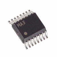
MAX11610EEE+ Maxim Integrated Products, MAX11610EEE+ Datasheet - Page 10

MAX11610EEE+
Manufacturer Part Number
MAX11610EEE+
Description
IC ADC SERIAL 10BIT 12CH 16-QSOP
Manufacturer
Maxim Integrated Products
Datasheet
1.MAX11607EUA.pdf
(22 pages)
Specifications of MAX11610EEE+
Number Of Bits
10
Sampling Rate (per Second)
94.4k
Data Interface
I²C, Serial
Number Of Converters
1
Power Dissipation (max)
3.35mW
Voltage Supply Source
Single Supply
Operating Temperature
-40°C ~ 85°C
Mounting Type
Surface Mount
Package / Case
16-SSOP (0.150", 3.90mm Width)
Resolution
10 bit
Interface Type
I2C
Snr
60 dB
Voltage Reference
4.096 V
Supply Voltage (max)
5.5 V
Supply Voltage (min)
4.5 V
Maximum Power Dissipation
666.7 mW
Maximum Operating Temperature
+ 85 C
Mounting Style
SMD/SMT
Input Voltage
5 V
Minimum Operating Temperature
- 40 C
Lead Free Status / RoHS Status
Lead free / RoHS Compliant
signal. At the end of the acquisition interval, the T/H
switches move to the hold position retaining the charge
on C
During the conversion interval, the switched capacitive
DAC adjusts to restore the comparator input voltage to
0V within the limits of 10-bit resolution. This action
requires 10 conversion clock cycles and is equivalent
to transferring a charge of 11pF
C
digital representation of the analog input signal.
Sufficiently low source impedance is required to ensure
an accurate sample. A source impedance of up to 1.5kΩ
does not significantly degrade sampling accuracy. To
minimize sampling errors with higher source impedances,
connect a 100pF capacitor from the analog input to GND.
This input capacitor forms an RC filter with the source
impedance limiting the analog-input bandwidth. For larg-
er source impedances, use a buffer amplifier to maintain
analog-input signal integrity and bandwidth.
When operating in internal clock mode, the T/H circuitry
enters its tracking mode on the eighth rising clock edge
of the address byte (see the Slave Address section). The
T/H circuitry enters hold mode on the falling clock edge of
the acknowledge bit of the address byte (the ninth clock
pulse). A conversion or a series of conversions is then
internally clocked and the MAX11606–MAX11611 holds
SCL low. With external clock mode, the T/H circuitry
enters track mode after a valid address on the rising
edge of the clock during the read (R/W = 1) bit. Hold
mode is then entered on the rising edge of the second
Low-Power, 4-/8-/12-Channel, I
10-Bit ADCs in Ultra-Small Packages
Figure 4. Equivalent Input Circuit
10
T/H
T/H
______________________________________________________________________________________
to the binary weighted capacitive DAC, forming a
as a stable sample of the input signal.
AIN3/REF
AIN0
AIN1
AIN2
GND
ANALOG INPUT MUX
(V
IN+
- V
IN-
) from
C
C
T/H
T/H
clock pulse during the shifting out of the first byte of the
result. The conversion is performed during the next 10
clock cycles.
The time required for the T/H circuitry to acquire an
input signal is a function of the input sample capaci-
tance. If the analog-input source impedance is high,
the acquisition time constant lengthens and more time
must be allowed between conversions. The acquisition
time (t
to be acquired. It is calculated by:
where R
R
clock mode and t
The MAX11606–MAX11611 feature input-tracking cir-
cuitry with a 5MHz small-signal bandwidth. The 5MHz
input bandwidth makes it possible to digitize high-
speed transient events and measure periodic signals
with bandwidths exceeding the ADC’s sampling rate by
using under sampling techniques. To avoid high-fre-
quency signals being aliased into the frequency band
of interest, anti-alias filtering is recommended.
Internal protection diodes clamp the analog input to
V
IN
DD
= 2.5kΩ, and C
and GND. These diodes allow the analog inputs to
ACQ
SOURCE
Analog Input Range and Protection
) is the minimum time needed for the signal
t
ACQ
V
DD
2
/2
C,
≥ 9
ACQ
is the analog-input source impedance,
REF
REF
IN
= 22pF. t
= 2/f
CAPACITIVE
DAC
CAPACITIVE
DAC
(R
SOURCE
Analog Input Bandwidth
SCL
for external clock mode.
ACQ
MAX11606
MAX11607
+ R
is 1.5/f
IN
)
SCL
C
IN
for internal


