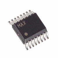
MAX11610EEE+ Maxim Integrated Products, MAX11610EEE+ Datasheet - Page 18

MAX11610EEE+
Manufacturer Part Number
MAX11610EEE+
Description
IC ADC SERIAL 10BIT 12CH 16-QSOP
Manufacturer
Maxim Integrated Products
Datasheet
1.MAX11607EUA.pdf
(22 pages)
Specifications of MAX11610EEE+
Number Of Bits
10
Sampling Rate (per Second)
94.4k
Data Interface
I²C, Serial
Number Of Converters
1
Power Dissipation (max)
3.35mW
Voltage Supply Source
Single Supply
Operating Temperature
-40°C ~ 85°C
Mounting Type
Surface Mount
Package / Case
16-SSOP (0.150", 3.90mm Width)
Resolution
10 bit
Interface Type
I2C
Snr
60 dB
Voltage Reference
4.096 V
Supply Voltage (max)
5.5 V
Supply Voltage (min)
4.5 V
Maximum Power Dissipation
666.7 mW
Maximum Operating Temperature
+ 85 C
Mounting Style
SMD/SMT
Input Voltage
5 V
Minimum Operating Temperature
- 40 C
Lead Free Status / RoHS Status
Lead free / RoHS Compliant
using an external reference or V
analog circuitry is inactive in shutdown and supply cur-
rent is less than 0.5µA (typ). The digital conversion
results obtained in internal clock mode are maintained
in memory during shutdown and are available for
access through the serial interface at any time prior to a
STOP or a repeated START condition.
When idle, the MAX11606–MAX11611 continuously wait
for a START condition followed by their slave address (see
Slave Address section). Upon reading a valid address
byte the MAX11606–MAX11611 power-up. The internal
reference requires 10ms to wake up, so when using the
internal reference it should be powered up 10ms prior to
conversion or powered continuously. Wake-up is invisible
when using an external reference or V
Automatic shutdown results in dramatic power savings,
particularly at slow conversion rates and with internal
clock. For example, at a conversion rate of 10ksps, the
average supply current for the MAX11607 is 60µA (typ)
and drops to 6µA (typ) at 1ksps. At 0.1ksps the average
supply current is just 1µA, or a minuscule 3µW of power
consumption, see Average Supply Current vs. Conversion
Rate in the Typical Operating Characteristics ).
SEL[2:0] of the setup byte (Table 1) control the reference
and the AIN_/REF configuration (Table 6). When
AIN_/REF is configured to be a reference input or refer-
ence output (SEL1 = 1), differential conversions on
AIN_/REF appear as if AIN_/REF is connected to GND
(see note 2 of Table 4). Single-ended conversion in scan
mode on AIN_/REF is ignored by internal limiter, which
sets the highest available channel at AIN2 or AIN10.
Low-Power, 4-/8-/12-Channel, I
10-Bit ADCs in Ultra-Small Packages
Table 6. Reference Voltage, AIN_/REF, and REF Format
X = Don’t care.
18
SEL2
______________________________________________________________________________________
0
0
1
1
1
1
SEL1
0
1
0
0
1
1
SEL0
X
X
0
1
0
1
Reference Voltage
DD
DD
External reference
Internal reference
Internal reference
Internal reference
Internal reference
as a reference, all
REFERENCE
as the reference.
VOLTAGE
V
DD
Reference output
Reference output
Reference input
Analog input
Analog input
Analog input
(MAX11606/
MAX11607/
MAX11610/
MAX11611)
AIN_/REF
The internal reference is 4.096V for the MAX11606/
MAX11608/MAX11610 and 2.048V for the MAX11607/
MAX11609/MAX11611. SEL1 of the setup byte controls
whether AIN_/REF is used for an analog input or a refer-
ence (Table 6). When AIN_/REF is configured to be an
internal reference output (SEL[2:1] = 11), decouple
AIN_/REF to GND with a 0.1µF capacitor and a 2kΩ series
resistor (see the Typical Operating Circuit ). Once powered
up, the reference always remains on until reconfigured.
The internal reference requires 10ms to wake up and is
accessed using SEL0 (Table 6). When in shutdown, the
internal reference output is in a high-impedance state. The
reference should not be used to supply current for exter-
nal circuitry. The internal reference does not require an
Figure 12. Unipolar Transfer Function
11 . . . 111
11 . . . 110
11 . . . 101
00 . . . 011
00 . . . 010
00 . . . 001
00 . . . 000
OUTPUT CODE
2
0
C,
1
Reference output
Reference output
Reference input
Not connected
Not connected
Not connected
2
INPUT VOLTAGE (LSB)
(MAX11608/
MAX11609)
3
REF
FULL-SCALE
TRANSITION
Internal Reference
REFERENCE STATE
FS - 3/2 LSB
MAX11606–
MAX11611
INTERNAL
Always off
Always off
Always off
Always on
Always off
Always on
1 LSB =
FS = V
ZS = GND
FS
REF
1024
V
REF


