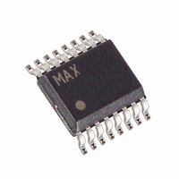
MAX11610EEE+ Maxim Integrated Products, MAX11610EEE+ Datasheet - Page 9

MAX11610EEE+
Manufacturer Part Number
MAX11610EEE+
Description
IC ADC SERIAL 10BIT 12CH 16-QSOP
Manufacturer
Maxim Integrated Products
Datasheet
1.MAX11607EUA.pdf
(22 pages)
Specifications of MAX11610EEE+
Number Of Bits
10
Sampling Rate (per Second)
94.4k
Data Interface
I²C, Serial
Number Of Converters
1
Power Dissipation (max)
3.35mW
Voltage Supply Source
Single Supply
Operating Temperature
-40°C ~ 85°C
Mounting Type
Surface Mount
Package / Case
16-SSOP (0.150", 3.90mm Width)
Resolution
10 bit
Interface Type
I2C
Snr
60 dB
Voltage Reference
4.096 V
Supply Voltage (max)
5.5 V
Supply Voltage (min)
4.5 V
Maximum Power Dissipation
666.7 mW
Maximum Operating Temperature
+ 85 C
Mounting Style
SMD/SMT
Input Voltage
5 V
Minimum Operating Temperature
- 40 C
Lead Free Status / RoHS Status
Lead free / RoHS Compliant
Figure 2. MAX11610/MAX11611 Functional Diagram
Figure 3. Load Circuit
The MAX11606–MAX11611 analog-to-digital converters
(ADCs) use successive-approximation conversion tech-
niques and fully differential input track/hold (T/H) cir-
cuitry to capture and convert an analog signal to a
serial 12-bit digital output. The MAX11606/MAX11607
are 4-channel ADCs, the MAX11608/MAX11609 are
8-channel ADCs, and the MAX11610/MAX11611 are
12-channel ADCs. These devices feature a high-speed
2-wire serial interface supporting data rates up to
SDA
_______________________________________________________________________________________
Detailed Description
V
AIN11/REF
DD
10-Bit ADCs in Ultra-Small Packages
AIN10
I
I
AIN0
AIN1
AIN2
AIN3
AIN4
AIN5
AIN6
AIN7
AIN8
AIN9
GND
SDA
OL
OH
SCL
V
DD
400pF
Low-Power, 4-/8-/12-Channel, I
V
OUT
CONFIGURATION REGISTER
ANALOG
INPUT
MUX
INPUT SHIFT REGISTER
SETUP REGISTER
REF
4.096V (MAX11610)
2.048V (MAX11611)
T/H
REFERENCE
10-BIT
ADC
1.7MHz. Figure 2 shows the simplified internal structure
for the MAX11610/MAX11611.
The MAX11606–MAX11611 operates from a single sup-
ply and consumes 670µA (typ) at sampling rates up to
94.4ksps. The MAX11607/MAX11609/MAX11611 feature
a 2.048V internal reference and the MAX11606/
MAX11608/MAX11610 feature a 4.096V internal refer-
ence. All devices can be configured for use with an
external reference from 1V to V
The MAX11606–MAX11611 analog-input architecture
contains an analog-input multiplexer (mux), a fully dif-
ferential track-and-hold (T/H) capacitor, T/H switches, a
comparator, and a fully differential switched capacitive
digital-to-analog converter (DAC) (Figure 4).
In single-ended mode, the analog-input multiplexer con-
nects C
CS[3:0] (see the Configuration/Setup Bytes (Write
Cycle) section) and GND (Table 3). In differential mode,
the analog- input multiplexer connects C
- analog inputs selected by CS[3:0] (Table 4).
During the acquisition interval, the T/H switches are in
the track position and C
CONTROL
LOGIC
T/H
MAX11610
MAX11611
OSCILLATOR
between the analog input selected by
INTERNAL
OUTPUT SHIFT
REGISTER
AND RAM
Analog Input and Track/Hold
T/H
charges to the analog input
DD
.
Power Supply
T/H
to the + and
2
C,
9


