LTC2442IG#PBF Linear Technology, LTC2442IG#PBF Datasheet - Page 19
LTC2442IG#PBF
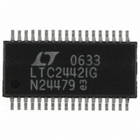
Manufacturer Part Number
LTC2442IG#PBF
Description
IC ADC 24BIT 4CH 36-SSOP
Manufacturer
Linear Technology
Datasheet
1.LTC2442CGPBF.pdf
(32 pages)
Specifications of LTC2442IG#PBF
Number Of Bits
24
Sampling Rate (per Second)
8k
Data Interface
MICROWIRE™, Serial, SPI™
Number Of Converters
1
Power Dissipation (max)
50mW
Voltage Supply Source
Single Supply
Operating Temperature
-40°C ~ 85°C
Mounting Type
Surface Mount
Package / Case
36-SSOP (0.200", 5.30mm Width)
Lead Free Status / RoHS Status
Lead free / RoHS Compliant
Available stocks
Company
Part Number
Manufacturer
Quantity
Price


Internal Serial Clock, Single Cycle Operation
This timing mode uses an internal serial clock to shift out
the conversion result and a CS signal to monitor and control
the state of the conversion cycle, see Figure 7.
In order to select the internal serial clock timing mode,
the EXT pin must be tied HIGH.
The serial data output pin (SDO) is Hi-Z as long as CS is
HIGH. At any time during the conversion cycle, CS may be
pulled LOW in order to monitor the state of the converter.
Once CS is pulled LOW, SCK goes LOW and EOC is output
to the SDO pin. EOC = 1 while a conversion is in progress
and EOC = 0 if the device is in the sleep state. Alterna-
tively, BUSY (Pin 2) may be used to monitor the status
of the conversion in progress. BUSY is HIGH during the
APPLICATIO S I FOR ATIO
BUSY
SCK
SDO
SDI
CS
CONVERSION
TEST EOC
U
TEST EOC
DON'T CARE
SLEEP
U
<t
Hi-Z
EOC(TEST)
1
BIT 31
EOC
1
Figure 7. Internal Serial Clock, Single Cycle Operation
W
2
BIT 30
“0”
0
3
BIT 29
SIG
EN
REFERENCE
0.1V TO V
ANALOG
INPUTS
VOLTAGE
0.1µF
0.1µF
4
BIT 28 BIT 27 BIT 26 BIT 25 BIT 24 BIT 23 BIT 22 BIT 21
MSB
SGL
1µF
4.5V TO 5.5V
U
CC
5
ODD
29
30
31
28
12
13
11
17
18
10
6
7
8
9
V
REF
REF
CH0
CH1
CH2
CH3
COM
OUTA
–INA
ADCINA
OUTB
–INB
ADCINB
6
CC
+
–
0
LTC2442
7
MUXOUTA
MUXOUTB
0
BUSY
+INA
+INB
GND
SDO
conversion and goes LOW at the conclusion. It remains
LOW until the result is read from the device.
When testing EOC, if the conversion is complete (EOC =
0), the device will exit the sleep state and enter the data
output state if CS remains LOW. In order to prevent the
device from exiting the sleep state, CS must be pulled
HIGH before the fi rst rising edge of SCK. In the internal
SCK timing mode, SCK goes HIGH and the device begins
outputting data at time t
(if EOC = 0) or t
during the falling edge of EOC). The value of t
500ns. If CS is pulled HIGH before time t
remains in the sleep state. The conversion result is held
in the internal static shift register.
SCK
EXT
SDI
CS
V
F
V
8
O
+
–
DATA OUTPUT
V
A0
21
27
25
26
19
24
4, 5, 32
CC
33
36
35
34
TO 15V
3
1
2
9
OSR3
–15V TO GND
1µF
V
CC
4-WIRE
SPI INTERFACE
10
OSR2
= EXTERNAL OSCILLATOR
= INTERNAL OSCILLATOR
(SIMULTANEOUS 50Hz/60Hz
REJECTION AT 6.9Hz OUTPUT RATE
11
OSR1
EOCtest
12
BIT 20 BIT 19
OSR0 TWOX
13
after EOC goes LOW (if CS is LOW
EOCtest
14
DON'T CARE
after the falling edge of CS
32
BIT 0
LSB
LTC2442
EOCtest
CONVERSION
Hi-Z
, the device
2442 F07
EOCtest
19
2442f
is
Related parts for LTC2442IG#PBF
Image
Part Number
Description
Manufacturer
Datasheet
Request
R

Part Number:
Description:
CD ROM LINEARVIEW DATASHEETS
Manufacturer:
Linear Technology

Part Number:
Description:
Standalone Linear Li-Ion Battery Charger with Thermal Regulation in ThinSOT
Manufacturer:
Linear Technology Corporation
Datasheet:
Part Number:
Description:
Low noise, high frequency, 8th order linear phase lowpass filter
Manufacturer:
Linear Technology Corporation
Datasheet:
Part Number:
Description:
Manufacturer:
Linear Technology Corporation
Datasheet:
Part Number:
Description:
Manufacturer:
Linear Technology Corporation
Datasheet:
Part Number:
Description:
Manufacturer:
Linear Technology Corporation
Datasheet:
Part Number:
Description:
Manufacturer:
Linear Technology Corporation
Datasheet:
Part Number:
Description:
Manufacturer:
Linear Technology Corporation
Datasheet:
Part Number:
Description:
Manufacturer:
Linear Technology Corporation
Datasheet:
Part Number:
Description:
Manufacturer:
Linear Technology Corporation
Datasheet:
Part Number:
Description:
Dual and Quad, JFET Input Precision High Speed Op Amps
Manufacturer:
Linear Technology Corporation
Datasheet:
Part Number:
Description:
Manufacturer:
Linear Technology Corporation
Datasheet:
Part Number:
Description:
1, 2, 6 and 8 Channel, 10-Bit Serial I/O Data Acquisition Systems
Manufacturer:
Linear Technology Corporation
Datasheet:
Part Number:
Description:
Manufacturer:
Linear Technology Corporation
Datasheet:
Part Number:
Description:
Universal dual filter building block
Manufacturer:
Linear Technology Corporation
Datasheet: