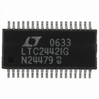
LTC2442IG#PBF Linear Technology, LTC2442IG#PBF Datasheet - Page 24

LTC2442IG#PBF
Manufacturer Part Number
LTC2442IG#PBF
Description
IC ADC 24BIT 4CH 36-SSOP
Manufacturer
Linear Technology
Datasheet
1.LTC2442CGPBF.pdf
(32 pages)
Specifications of LTC2442IG#PBF
Number Of Bits
24
Sampling Rate (per Second)
8k
Data Interface
MICROWIRE™, Serial, SPI™
Number Of Converters
1
Power Dissipation (max)
50mW
Voltage Supply Source
Single Supply
Operating Temperature
-40°C ~ 85°C
Mounting Type
Surface Mount
Package / Case
36-SSOP (0.200", 5.30mm Width)
Lead Free Status / RoHS Status
Lead free / RoHS Compliant
Available stocks
Company
Part Number
Manufacturer
Quantity
Price
LTC2442
Input Bandwidth and Frequency Rejection
The combined effect of the internal SINC
the digital and analog autocalibration circuits determines
the LTC2442 input bandwidth and rejection characteristics.
The digital fi lter’s response can be adjusted by setting the
oversample ratio (OSR) through the SPI interface or by
supplying an external conversion clock to the f
Table 7 lists the properties of the LTC2442 with various
combinations of oversample ratio and clock frequency.
Understanding these properties is the key to fi ne tuning
the characteristics of the LTC2442 to the application.
Maximum Conversion Rate
The maximum conversion rate is the fastest possible rate
at which conversions can be performed.
APPLICATIO S I FOR ATIO
24
Table 7
*ADC noise increases by approximately √2 when OSR is decreased by a factor of 2 for OSR 32768 to OSR 256. The ADC noise at OSR 64 include effects
from internal modulator quantization noise.
sample
(OSR)
16384
32768
Over-
Ratio
1024
2048
4096
8192
128
256
512
64
840nV
630nV
430nV
305nV
220nV
*RMS
Noise
3.6µV
2.1µV
1.5µV
1.2µV
23µV
U
(V
REF
ENOB
17.7
20.4
21.2
21.6
22.5
22.4
23.5
24.4
22
24
U
= 5V)
ANALOG INPUT
0.1V TO V
–0.5V
REFERENCE
VOLTAGE
9MHz clock
0.5V
Internal
REF
3515.6
1757.8
1µF
878.9
439.5
219.7
109.9
4.5V TO 5.5V
W
54.9
27.5
13.7
REF
Conversion Rate
6.9
TO
CC
4,5,32
Maximum
4
29
30
31
6
7
digital fi lter and
Figure 14. Simple External Clock Source
V
REF
REF
CH0
CH1
GND
CC
f
•
•
•
f
f
f
0
LTC2442
f
f
f
f
External
0
0
0
+
–
/1310720
f
f
0
0
0
0
/163840
/327680
/655360
0
0
/10240
/20480
/40960
/81920
/2560
/5120
O
U
f
0
BUSY
pin.
SDO
SCK
EXT
CS
F
O
2
34
1
36
35
3
9MHz clock
14062.5
Internal
7031.3
3515.6
1757.8
28125
878.9
439.5
219.7
109.9
54.9
3-WIRE
SPI INTERFACE
First Notch
Frequency
First Notch Frequency
This is the fi rst notch in the SINC
and depends on the fo clock frequency and the oversample
ratio. Rejection at this frequency and its multiples (up to
the modulator sample rate of 1.8MHz) exceeds 120dB.
This is 8 times the maximum conversion rate.
Effective Noise Bandwidth
The LTC2442 has extremely good input noise rejection from
the fi rst notch frequency all the way out to the modulator
sample rate (typically 1.8MHz). Effective noise bandwidth
is a measure of how the ADC will reject wideband input
noise up to the modulator sample rate
NC
External
f
f
f
f
f
f
f
f
0
f
f
0
0
0
0
0
0
0
/16380
0
0
/1280
/2560
/5120
/1020
/2050
/4100
/8190
OUT
DIV
/320
/640
f
0
LTC1799
GND
SET
V
9MHz clock
+
Internal
3148
1574
98.4
49.2
24.6
12.4
787
394
197
6.2
Noise BW
0.1µF
Effective
2442 F14
R
f
SET
f
f
f
0
External
f
f
f
f
f
f
0
0
0
/146300
0
0
0
0
0
0
/18300
/36600
/73100
/5710
/2860
/1140
/2280
/4570
/9140
f
0
4
portion of the digital fi lter
9MHz clock
Internal
1696
26.5
13.2
848
424
212
106
6.6
3.3
53
point (Hz)
–3dB
f
f
f
f
f
0
0
External
f
f
f
f
0
0
0
/1358000
/2717000
f
0
0
0
0
/170000
/340000
/679000
0
/10600
/21200
/42500
/84900
/5310
f
0
2442f


