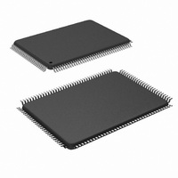
LM97593VH/NOPB National Semiconductor, LM97593VH/NOPB Datasheet - Page 41

LM97593VH/NOPB
Manufacturer Part Number
LM97593VH/NOPB
Description
IC DDC ADC/TUNER/AGC 128-PQFP
Manufacturer
National Semiconductor
Datasheet
1.LM97593VHNOPB.pdf
(50 pages)
Specifications of LM97593VH/NOPB
Number Of Bits
12
Sampling Rate (per Second)
65M
Data Interface
Serial
Number Of Converters
2
Power Dissipation (max)
560mW
Voltage Supply Source
Analog and Digital
Operating Temperature
-40°C ~ 85°C
Mounting Type
Surface Mount
Package / Case
128-BFQFP
Lead Free Status / RoHS Status
Lead free / RoHS Compliant
Other names
LM97593VH
Available stocks
Company
Part Number
Manufacturer
Quantity
Price
Company:
Part Number:
LM97593VH/NOPB
Manufacturer:
VK
Quantity:
1 980
Company:
Part Number:
LM97593VH/NOPB
Manufacturer:
Texas Instruments
Quantity:
10 000
AGC Theory of Operation
A block diagram of the AGC is shown in Figure 40. The DVGA
interface comprises four pins for each of the channels. The
first three pins of this interface are a 3-bit binary word that
controls the DVGA gain in 6dB steps (AGAIN). The final pin
is ASTROBE which allows the AGAIN bits to be latched into
the DVGA’s register. A key feature of the ASTROBE, illus-
trated Figure 41, is that it toggles only if the data on AGAIN
has changed from the previous cycle. Not shown is that AS-
TROBE and BSTROBE are independent. For example, AS-
TROBE
BSTROBE will not toggle because AGAIN has changed. This
is done to minimize unnecessary digital noise on the sensitive
analog path through the DVGA. ASTROBE and BSTROBE
are asserted during MR and SI to properly initialize the DV-
GAs.
The absolute value circuit and the 2-stage, decimate-by-8
CIC filter comprise the power detection part of the AGC. The
power detector bandwidth is set by the CIC filter to F
absolute value circuit doubles the effective input frequency.
This has the effect of reducing the power detector bandwidth
from F
For a full-scale sinusoidal input, the absolute value circuit
output is a dc value of 511*(2/
FIGURE 41. Timing diagram for AGC/DVGA interface, Channel A. Refer to Figure 7 for detailed timing information.
CK
/8 to F
only
CK
toggles
/16.
when
π
). Because the absolute value
AGAIN
FIGURE 40. LM97593 AGC circuit, Channel A
has
changed.
CK
/8. The
41
circuit also generates undesired even harmonic terms, the
CIC filter (response shown in Figure 39) is required to remove
these harmonics. The first response null occurs at
FIGURE 39. Power detector filter response, 52 MHz
30008738
www.national.com
30008737
30008736


